
Graphene Electrode Based Ceramic Capacitor

a ceramic capacitor and graphene electrode technology, applied in the field of ceramic capacitors, can solve the problems of inability to meet the requirements of a single atom of graphene, inability to meet the requirements of a single atom, so as to improve the crystal structure and physical properties of the graphene film

Active Publication Date: 2016-03-17
GLOBAL GRAPHENE GRP INC
View PDF3 Cites 50 Cited by
  • Summary
  • Abstract
  • Description
  • Claims
  • Application Information

AI Technical Summary

Benefits of technology

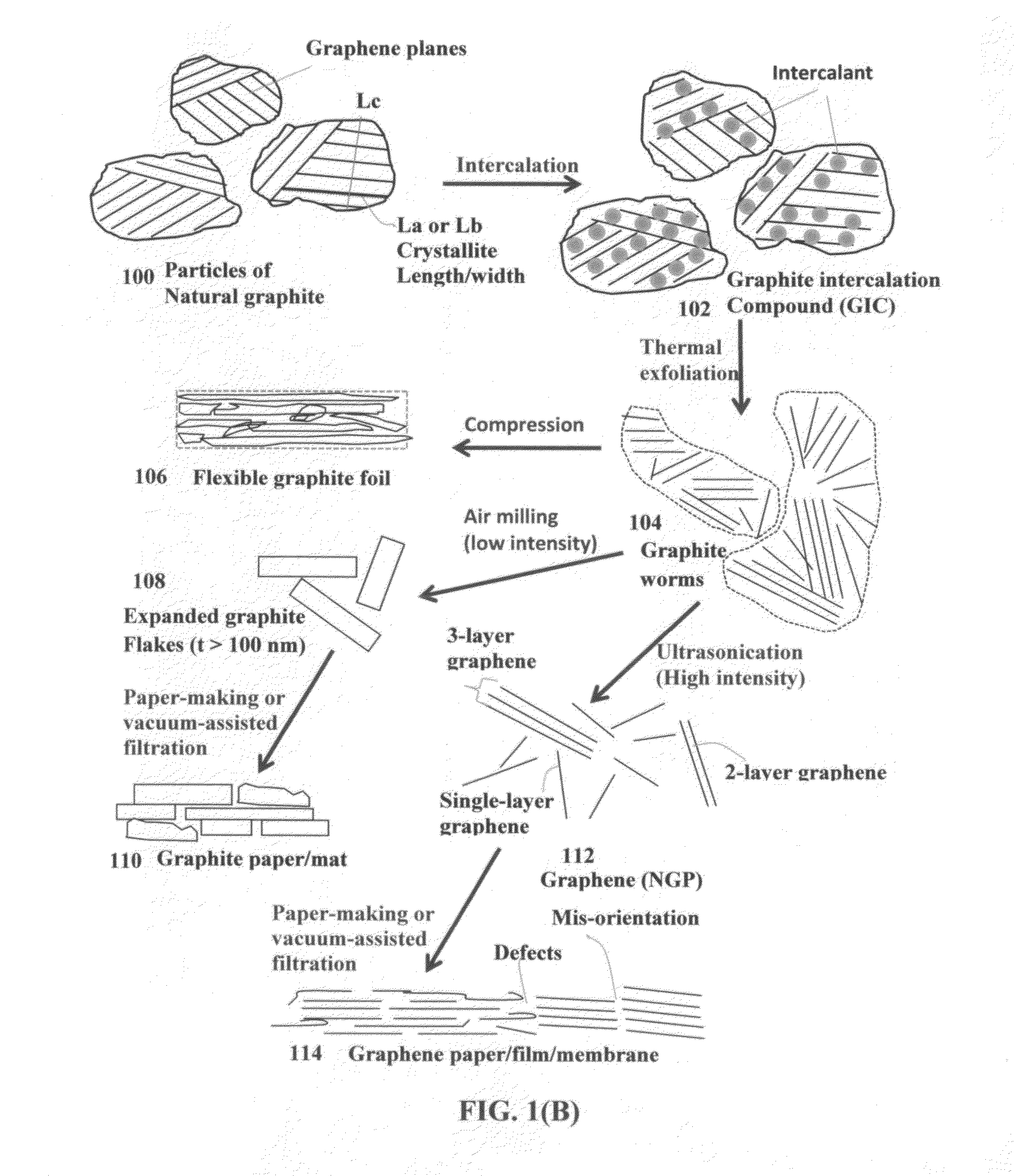
The present invention provides a ceramic capacitor with a graphene electrode layer. The graphene electrode layer is made of a layer of graphene or exfoliated graphite, which replaces metal electrodes in conventional ceramic capacitors. The thickness of the graphene electrode layer is at least 2 nm, which is necessary for reasonable handling. The graphene electrode layer can be made of a single-layer or multi-layer graphene, and it can contain discrete graphite flakes or exfoliated graphite flakes bonded by a binder material or dispersed in a matrix material. The graphene electrode layer can be directly deposited onto a ceramic layer using metal catalyzed chemical vapor deposition (CVD) or it can be made into a layer of graphene or exfoliated graphite by other methods such as chemical exfoliation or chemical vapor deposition (CVD) on a metal substrate. The invention provides a ceramic capacitor with improved performance and reliability.

Problems solved by technology

The CVD-made, ultra-thin film is too difficult to handle.
The CVD graphene film is typically deposited on a Cu / Ni surface and the graphene film must be detached from the Cu / Ni substrate (e.g. by chemically etching away Cu / Ni, an expensive, delicate, and environmentally non-benign procedure).

Method used


Image

  • Graphene Electrode Based Ceramic Capacitor
  • Graphene Electrode Based Ceramic Capacitor
  • Graphene Electrode Based Ceramic Capacitor

Examples


example 1

Preparation of Discrete Nano Graphene Platelets (NGPs) which are GO Sheets

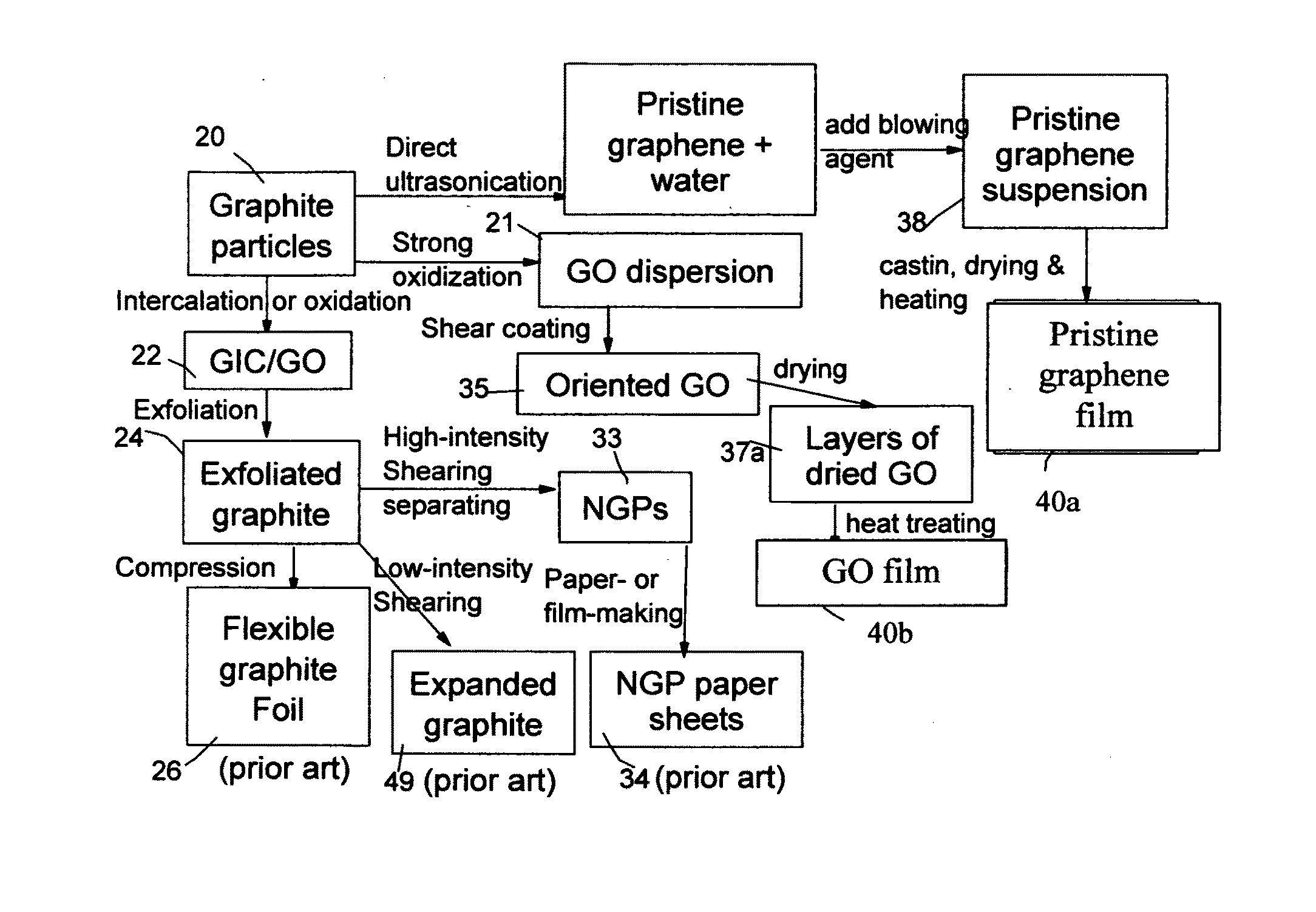
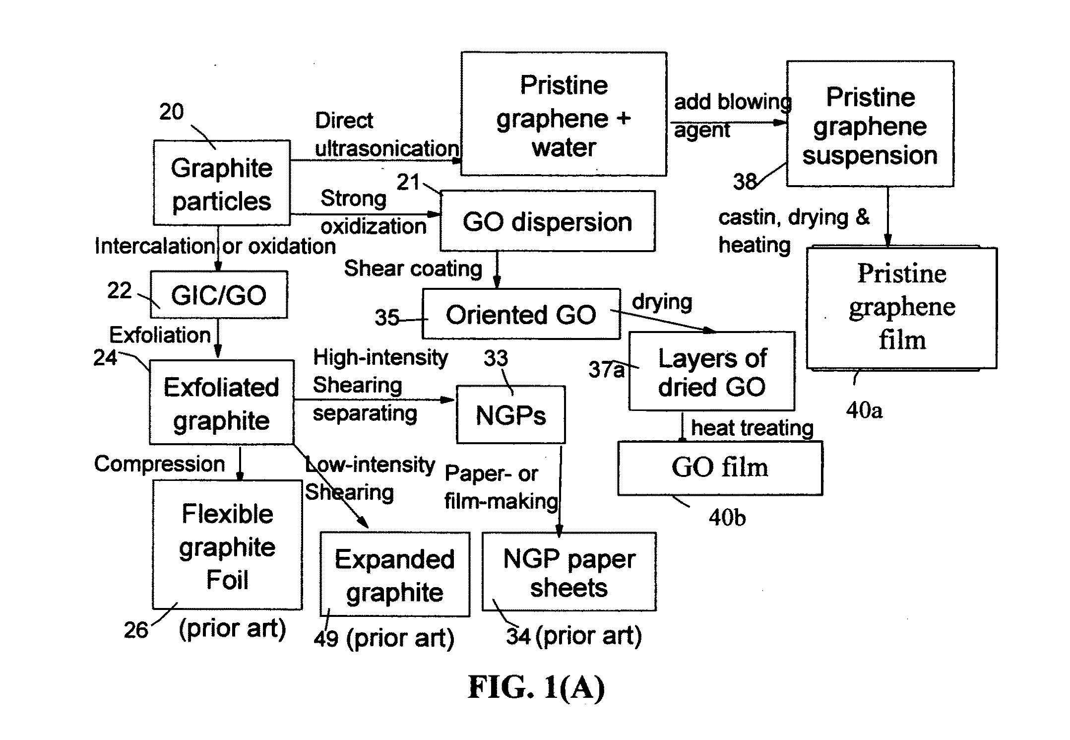
[0084]Chopped graphite fibers with an average diameter of 12 μm and natural graphite particles were separately used as a starting material, which was immersed in a mixture of concentrated sulfuric acid, nitric acid, and potassium permanganate (as the chemical intercalate and oxidizer) to prepare graphite intercalation compounds (GICs). The starting material was first dried in a vacuum oven for 24 h at 80° C. Then, a mixture of concentrated sulfuric acid, fuming nitric acid, and potassium permanganate (at a weight ratio of 4:1:0.05) was slowly added, under appropriate cooling and stirring, to a three-neck flask containing fiber segments. After 5-16 hours of reaction, the acid-treated graphite fibers or natural graphite particles were filtered and washed thoroughly with deionized water until the pH level of the solution reached 6. After being dried at 100° C. overnight, the resulting graphite intercalation compo...

example 2

Preparation of Single-Layer Graphene Sheets from Meso-Carbon Micro-Beads (MCMBs)

[0087]Meso-carbon microbeads (MCMBs) were supplied from China Steel Chemical Co., Kaohsiung, Taiwan. This material has a density of about 2.24 g / cm3 with a median particle size of about 16 μm. MCMB (10 grams) were intercalated with an acid solution (sulfuric acid, nitric acid, and potassium permanganate at a ratio of 4:1:0.05) for 48-96 hours. Upon completion of the reaction, the mixture was poured into deionized water and filtered. The intercalated MCMBs were repeatedly washed in a 5% solution of HCl to remove most of the sulphate ions. The sample was then washed repeatedly with deionized water until the pH of the filtrate was no less than 4.5. The slurry was then subjected ultrasonication for 10-100 minutes to produce GO suspensions. TEM and atomic force microscopic studies indicate that most of the GO sheets were single-layer graphene when the oxidation treatment exceeded 72 hours, and 2- or 3-layer g...

example 3

Preparation of Pristine Graphene Film (0% Oxygen)

[0090]Recognizing the possibility of the high defect population in GO sheets acting to reduce the conductivity of individual graphene plane, we decided to study if the use of pristine graphene sheets (non-oxidized and oxygen-free, non-halogenated and halogen-free, etc.) can lead to a graphene film having a higher thermal conductivity. Pristine graphene sheets were produced by using the direct ultrasonication or liquid-phase production process. In a typical procedure, five grams of graphite flakes, ground to approximately 20 μm or less in sizes, were dispersed in 1,000 mL of deionized water (containing 0.1% by weight of a dispersing agent, Zonyl® FSO from DuPont) to obtain a suspension. An ultrasonic energy level of 85 W (Branson S450 Ultrasonicator) was used for exfoliation, separation, and size reduction of graphene sheets for a period of 15 minutes to 2 hours. The resulting graphene sheets are pristine graphene that have never been ...


PUM

PropertyMeasurementUnit
thicknessaaaaaaaaaa
thicknessaaaaaaaaaa
thicknessaaaaaaaaaa

Abstract

A ceramic capacitor comprising at least a dielectric ceramic layer and at least a graphene electrode layer deposited on the ceramic layer, wherein the graphene electrode layer has a thickness no less than 2 nm and consists of a graphene material or a graphene composite material containing at least 0.1% by weight of a graphene material dispersed in a matrix material or bonded by a binder material, wherein the graphene material is selected from (a) a plurality of single-layer or multi-layer pristine graphene sheets having less than 0.01% by weight of non-carbon elements, or (b) one or a plurality of a non-pristine graphene material having at least 0.01% by weight of non-carbon elements, wherein the non-pristine graphene is selected from graphene oxide, reduced graphene oxide, graphene fluoride, graphene chloride, graphene bromide, graphene iodide, hydrogenated graphene, nitrogenated graphene, doped graphene, chemically functionalized graphene, or a combination thereof.

Description

FIELD OF THE INVENTION[0001]The present invention relates generally to the field of ceramic capacitor and, more particularly, to the ceramic capacitor containing a graphene-based material (instead of metal) as the primary electrode material. It may be noted that the ceramic capacitor is unrelated to the supercapacitor (also known as ultracapacitor or electrochemical capacitor) or the electrolytic capacitor. These three (ceramic capacitor, supercapacitor, and electrolytic capacitor) are fundamentally different and patently distinct classes of electronic devices.BACKGROUND OF THE INVENTION[0002]A ceramic capacitor, also referred to as a dielectric ceramic, is a capacitor in which a ceramic material acts as the dielectric and a metal as the electrode. Typically, a ceramic capacitor is constructed of two or more alternating layers of ceramic dielectric and metal. The composition of the ceramic material governs the electrical behaviors and, hence, applications of the resulting ceramic ca...

Claims


Application Information

Patent Timeline
Patent Type & Authority Applications(United States)
IPC IPC(8): H01G4/008C01B31/04C04B35/465H01G4/12
CPCH01G4/008H01G4/1227C04B35/465H01G4/1254C01B31/0438H01G4/1245B32B18/00C01B32/182C01B32/198C04B35/4682C04B35/6261C04B35/62675C04B35/62685C04B35/62695C04B35/634C04B35/638C04B2235/3215C04B2235/3217C04B2235/3224C04B2235/3227C04B2235/3236C04B2235/3244C04B2235/3262C04B2235/3272C04B2235/3275C04B2235/3279C04B2235/3281C04B2235/3284C04B2235/3418C04B2235/442C04B2235/6025C04B2235/6582C04B2235/79C04B2237/346C04B2237/68C04B2237/704
Inventor LIN, YI-JUNJANG, BOR ZLEE, SHAIO-YENZHAMU, ARUNA
Owner GLOBAL GRAPHENE GRP INC
Learn More