Ultra Long Lifetime Gallium Arsenide

a gallium arsenide and long-life technology, applied in the direction of polycrystalline material growth, crystal growth process, chemically reactive gas, etc., can solve the problems of high cost, high cost, and limited operation complexity of semiconductor radiation detectors, and achieve the effect of increasing the carrier lifetim

Active Publication Date: 2015-08-20
BAE SYST INFORMATION & ELECTRONICS SYST INTERGRATION INC
View PDF7 Cites 2 Cited by
  • Summary
  • Abstract
  • Description
  • Claims
  • Application Information

AI Technical Summary

Problems solved by technology

Commercially available GaAs always has a significant concentration of a defect called EL2 (As on Ga antisite defects) which are known to greatly reduce the free-carrier lifetime of the material.
Crystal growth from the vapor phase can be done at a temperature significantly lower than that of the melting point of the compound, however, most vapor growth techniques such as molecular organic chemical vapor deposition (MOCVD) and molecular beam epitaxy (MBE) have growth rates that are much too slow to make growth of any material approaching that of bulk quantities (>100 micrometers) impractical.
Historically, however, semiconductor radiation detectors have been limited by high cost, operational complexity, low efficiency due to limited size, and difficulty achieving high-purity, defect-free crystals.
Unfortunately, progress in overcoming these obstacles over the years has been slow and incremental.
Progress in the development of high resolution, room temperature, gamma radiation detectors has been severely limited for many years by the size, quality, and transport properties of single crystal of compound semiconductors.
CdxZn1-xTe (CZT) is the most commercially advanced of these materials, but Te inclusions, twins, and grain boundaries are constant barriers to the size, yield, and cost of these crystals for detector applications.
Gallium arsenide (GaAs) has been studied as a radiation detector since the early 1960's, predating CZT, but its widespread use for gamma ray detection has never been realized due to the presence of native deep level traps (EL2, i.e., AsGa antisites) which reduced its free carrier lifetime at room temperature.

Method used


Image

  • Ultra Long Lifetime Gallium Arsenide
  • Ultra Long Lifetime Gallium Arsenide
  • Ultra Long Lifetime Gallium Arsenide

Examples


Embodiment Construction

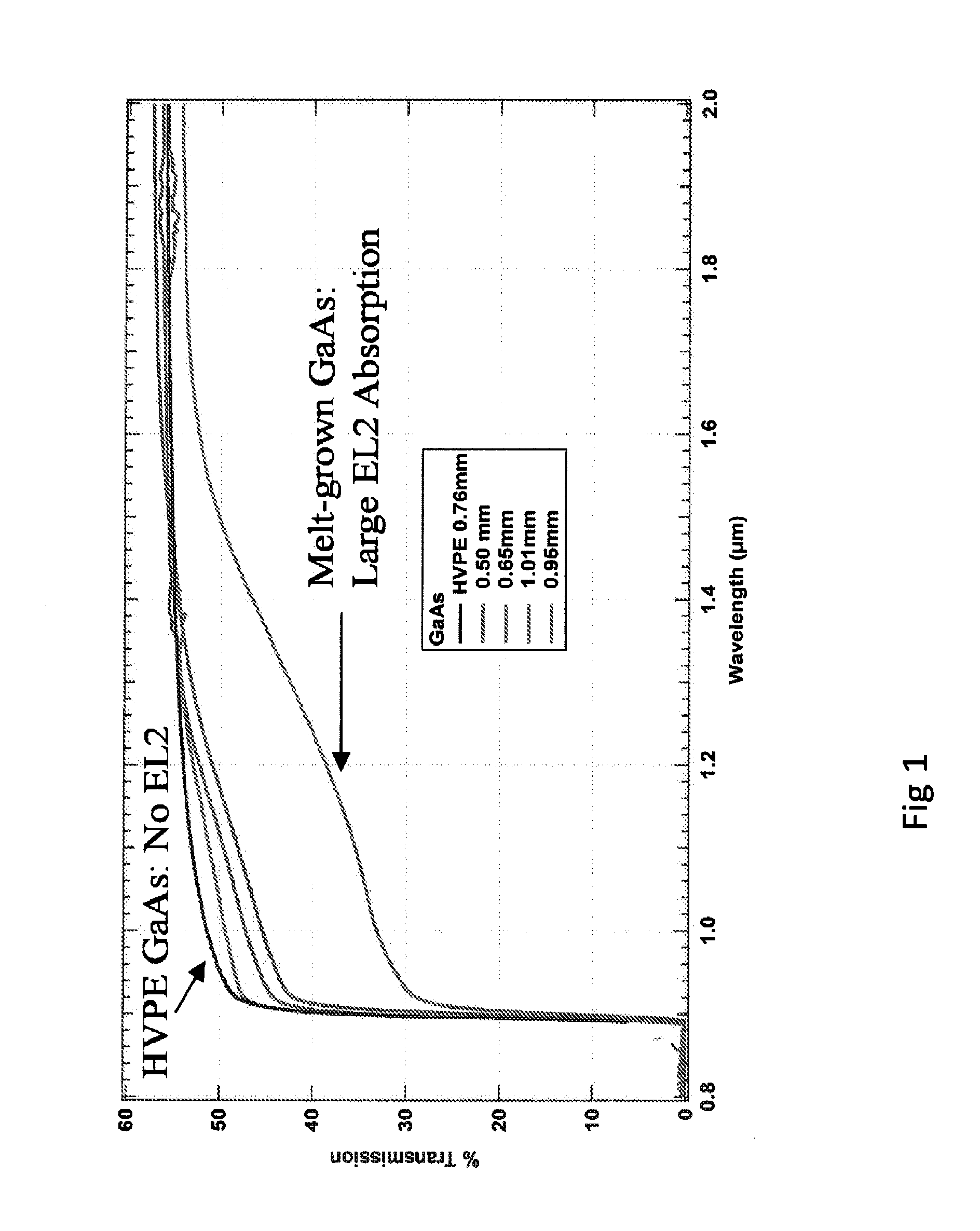
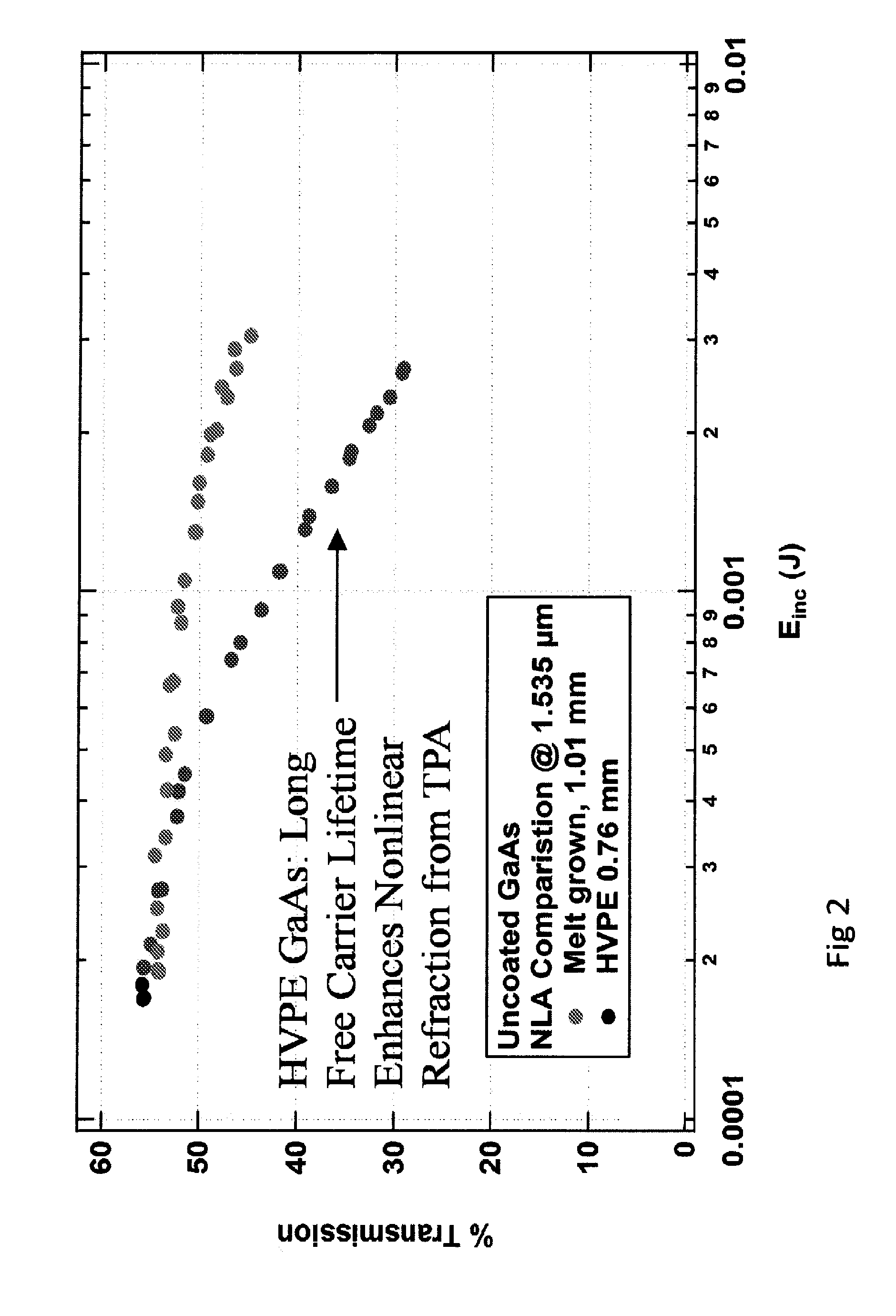
[0021]This preferred embodiment is a new GaAs with an increased carrier lifetime of at least 10 microseconds that can be used for optical devices, electrical devices and other devices. The preferred embodiment of a new GaAs is created using a known, but little-used, method of vapor growth of semiconductor crystals, low pressure hydride phase epitaxy (LP-HVPE), to produce GaAs with the unique properties of having ultra-long free carrier lifetimes. This method of fabricating the preferred embodiment of a new GaAs crystal significantly advances the state of the art of semiconductor materials for multiple applications, including high resolution radiation detectors, dramatically improves the material quality, and is scalable to production of large quantities and aperture sizes.

[0022]Data supporting the increased free-carrier lifetime of GaAs grown in the LP-HVPE reactor include optical transmission spectra data, two photon non-linear absorption data, microwave-photoconductive decay (μ-PC...


PUM

PropertyMeasurementUnit
thickaaaaaaaaaa
pressureaaaaaaaaaa
voltageaaaaaaaaaa

Abstract

A novel bulk GaAs with an increased carrier lifetime of at least 10 microseconds has been produced. This novel GaAs has many uses to improve optical and electrical devices. The method of producing the GaAs crystal involves using a technique called low pressure hydride phase epitaxy (LP-HVPE). In this technique, a gas containing Ga (typically GaCl) is reacted with a gas containing As (typically AsH3) at the surface of a GaAs substrate. When grown under the proper conditions, the epitaxial, vapor grown GaAs crystal has ultra-long free carrier lifetimes of at least one order of magnitude greater than that of the previous art of 1 microsecond. This very long free carrier lifetime GaAs will be particularly useful as a semiconductor radiation detector material and is also expected to be useful for many other applications than include medical imaging, solar cells, diode lasers, and optical limiters and other applications.

Description

BACKGROUND OF THE INVENTION[0001]1. Field of Invention[0002]The current invention relates generally to a new embodiment of bulk GaAs with an increased carrier lifetime of at least 10 microseconds to be used for optical and electrical devices. The invention also relates to the apparatus, systems and methods for creating GaAs with very long free carrier lifetimes. More particularly, this very long free carrier lifetime GaAs is expected to be useful as a semiconductor radiation detector material, and also is expected to be useful for applications including, but not limited to, medical imaging, solar cells, diode lasers, and optical limiters.[0003]2. Description of Related Art[0004]GaAs is a well-known semiconductor and is grown by many methods. It can be produced using a variety of techniques including both bulk melt growth and vapor growth. Commercially available GaAs always has a significant concentration of a defect called EL2 (As on Ga antisite defects) which are known to greatly r...

Claims


Application Information

Patent Timeline
Patent Type & Authority Applications(United States)
IPC IPC(8): H01L21/02C22C28/00
CPCC22C28/00C30B25/00C30B29/42H01L21/02395H01L21/02546H01L21/0262
Inventor SCHUNEMANN, PETER G.ZAWILSKI, KEVIN T.
Owner BAE SYST INFORMATION & ELECTRONICS SYST INTERGRATION INC
Why Eureka
Try Eureka