Photoelectric conversion element, method for using the same, imaging device, photosensor, and compound
- Summary
- Abstract
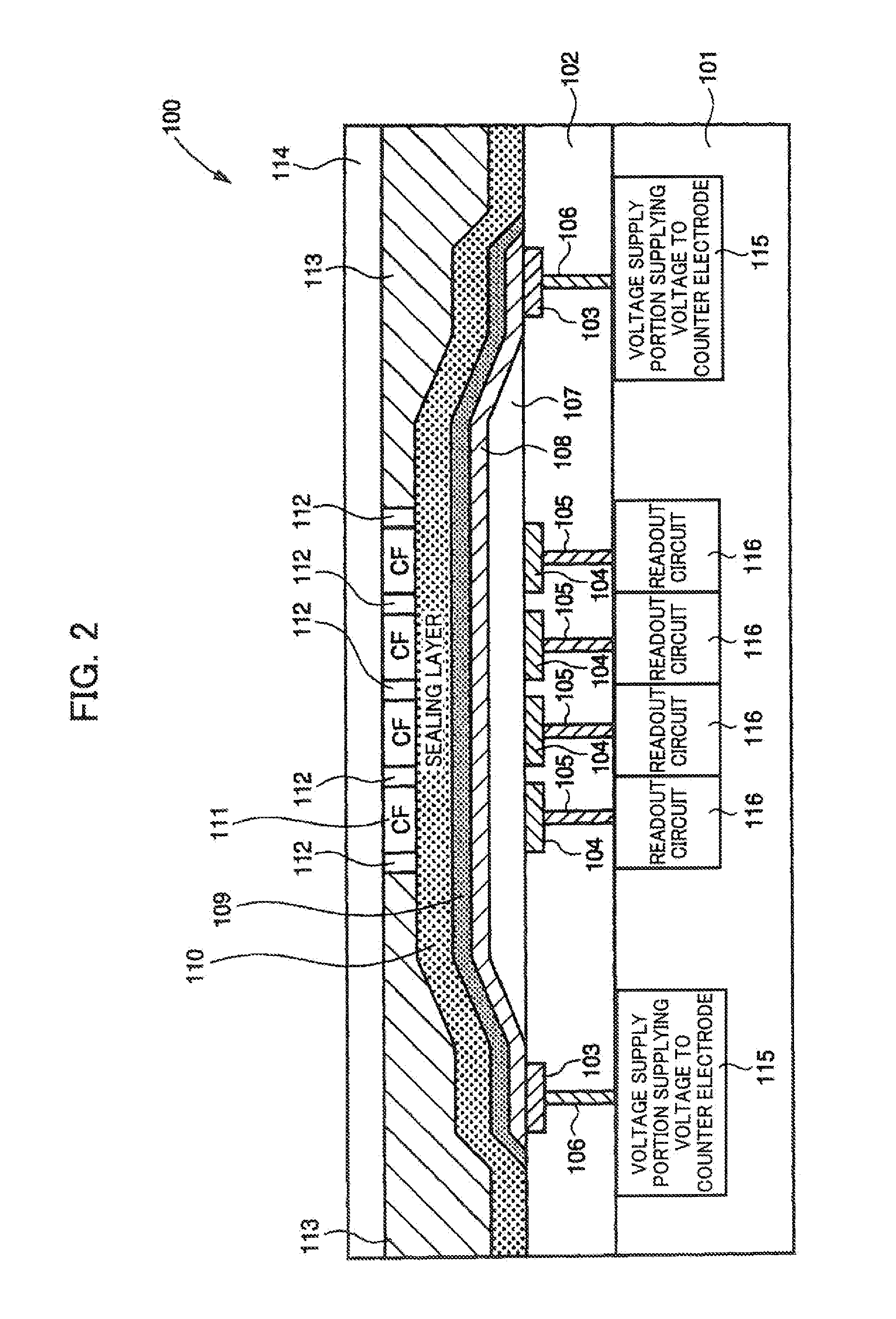
- Description
- Claims
- Application Information
AI Technical Summary
Benefits of technology
Problems solved by technology
Method used
Image


Examples
examples
[0252]Examples will be described below, but the present invention is not limited thereto.
[0253](Synthesis of Compound D1)
[0254]Sodium 4,5-dichlorophthalate (5.9 g, 23.0 mmol) and triethylamine (5.4 g, 53.0 mmol) were dissolved in 15 ml of acetic anhydride, and to the resultant solution, tert-butyl acetate (4.2 g, 26.5 mmol) was added dropwise. Thereafter, the solution was stirred for 2 hours at room temperature, thereby obtaining Compound 1. In a state where Compound 1 has not been isolated, 10 g of ice and 8 ml of 35% concentrated hydrochloric acid were directly added to the reaction mixture, and the resultant was heated and stirred for 30 minutes at 50° C., thereby obtaining Compound 2 at a yield of 83%.
[0255]2-iso-propenylaniline (4.20 g, 31.5 mmol), palladium acetate (210 mg, 0.95 mmol), tri(t-butyl)phosphine (570 mg, 2.80 mmol), cesium carbonate (20.5 g, 62.9 mmol), and methyl 6-bromo-2-naphthoate (8.35 g, 31.5 mmol) were dissolved in 50 ml of xylene and reacted under reflux at...
PUM
 Abstract
Description
Claims
Application Information
 - R&D Engineer
- R&D Manager
- IP Professional
- Industry Leading Data Capabilities
- Powerful AI technology
- Patent DNA Extraction
Browse by: Latest US Patents, China's latest patents, Technical Efficacy Thesaurus, Application Domain, Technology Topic.
© 2024 PatSnap. All rights reserved.Legal|Privacy policy|Modern Slavery Act Transparency Statement|Sitemap