
Timing calibration for on-chip interconnect

Active Publication Date: 2014-03-13
NVIDIA CORP
View PDF10 Cites 22 Cited by
  • Summary
  • Abstract
  • Description
  • Claims
  • Application Information

AI Technical Summary

Benefits of technology

The patent text describes a technique to calibrate timing for on-chip interconnects to reduce delays caused by wires. By doing so, chip yields can improve, meaning more chips can be made successfully.

Problems solved by technology

However as silicon die sizes increase, the on-chip interconnect may span 10 mm or more in length, and the communication channels are subject to many sources of timing error, including crosstalk, power-supply-induced jitter (PSIJ), and wire delay variation, due to transistor and wire metallization mismatch.
Power supply noise on the order of + / −7% can result in significant modulation of data rate (through modulation of signal propagation velocity), further reducing the effective timing margin by as much as 400 mUI.
In such harsh environments, wire delay mismatch can cause chips to fail to operate properly, as explained above regarding the transmission of the “lone 1”, resulting in severe yield loss.
The combination of wire delay mismatches, timing jitter, and power supply noise may reduce the effective timing margin such that clock frequency must be reduced to ensure that timing margin constraints are met so that the chip operates properly.
In particular, the chips may fail when an on-chip source-synchronous, CMOS-repeater-based interconnect serves as the building block for large on-chip networks responsible for moving several terabytes of data per second across large portions of the chip.
Failure of even a single signal transmitted on the wire of the interconnect to satisfy the timing margin constraints will likely result in a functional failure of the chip.
Delay mismatch among the various wires in a given sub-channel of the on-chip interconnect results in DCD and clock-to-data skew, reducing the yield.

Method used


Image

  • Timing calibration for on-chip interconnect
  • Timing calibration for on-chip interconnect
  • Timing calibration for on-chip interconnect

Examples


Embodiment Construction

[0032]In the following description, numerous specific details are set forth to provide a more thorough understanding of the present invention. However, it will be apparent to one of skill in the art that the present invention may be practiced without one or more of these specific details. In other instances, well-known features have not been described in order to avoid obscuring the present invention.

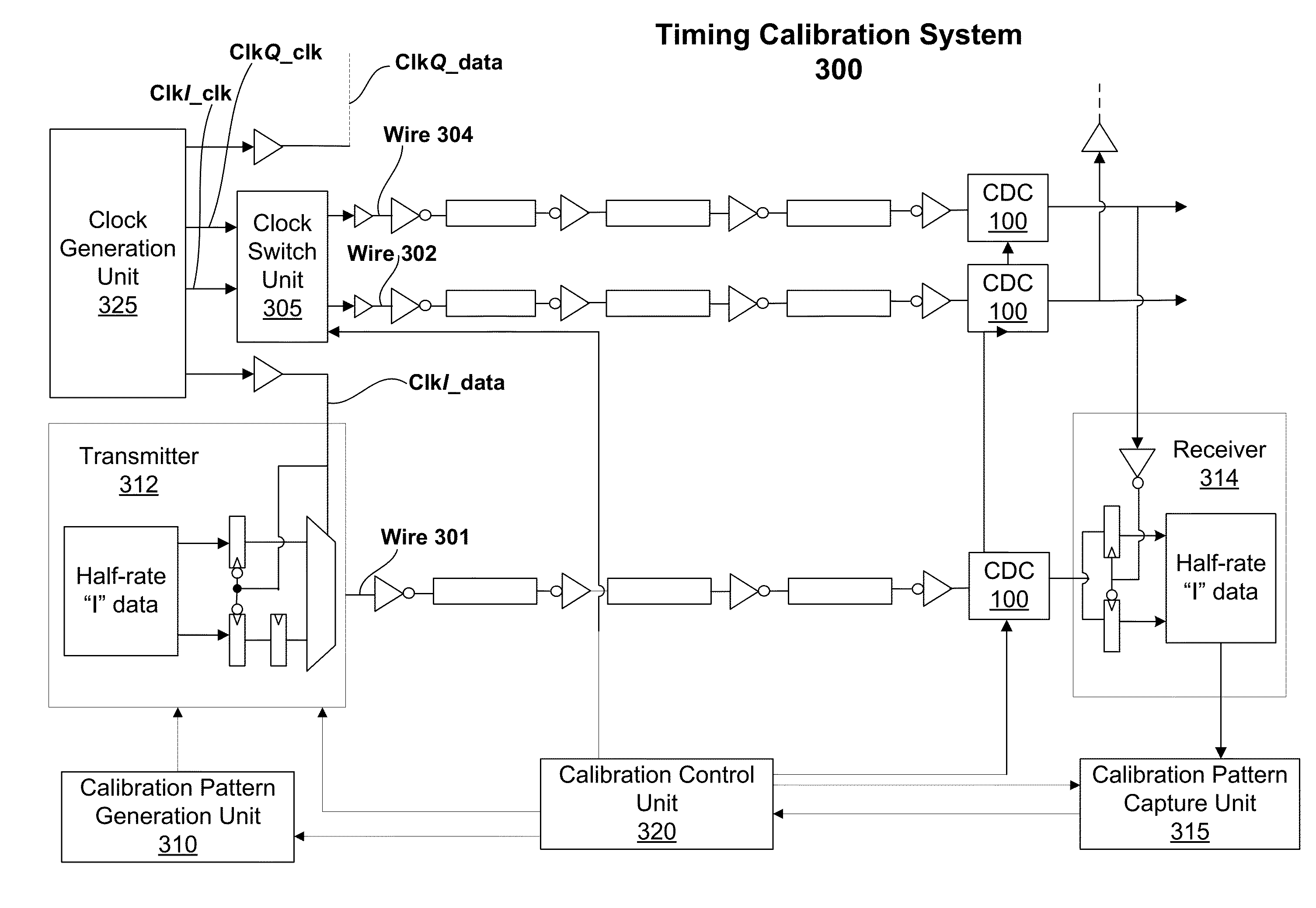
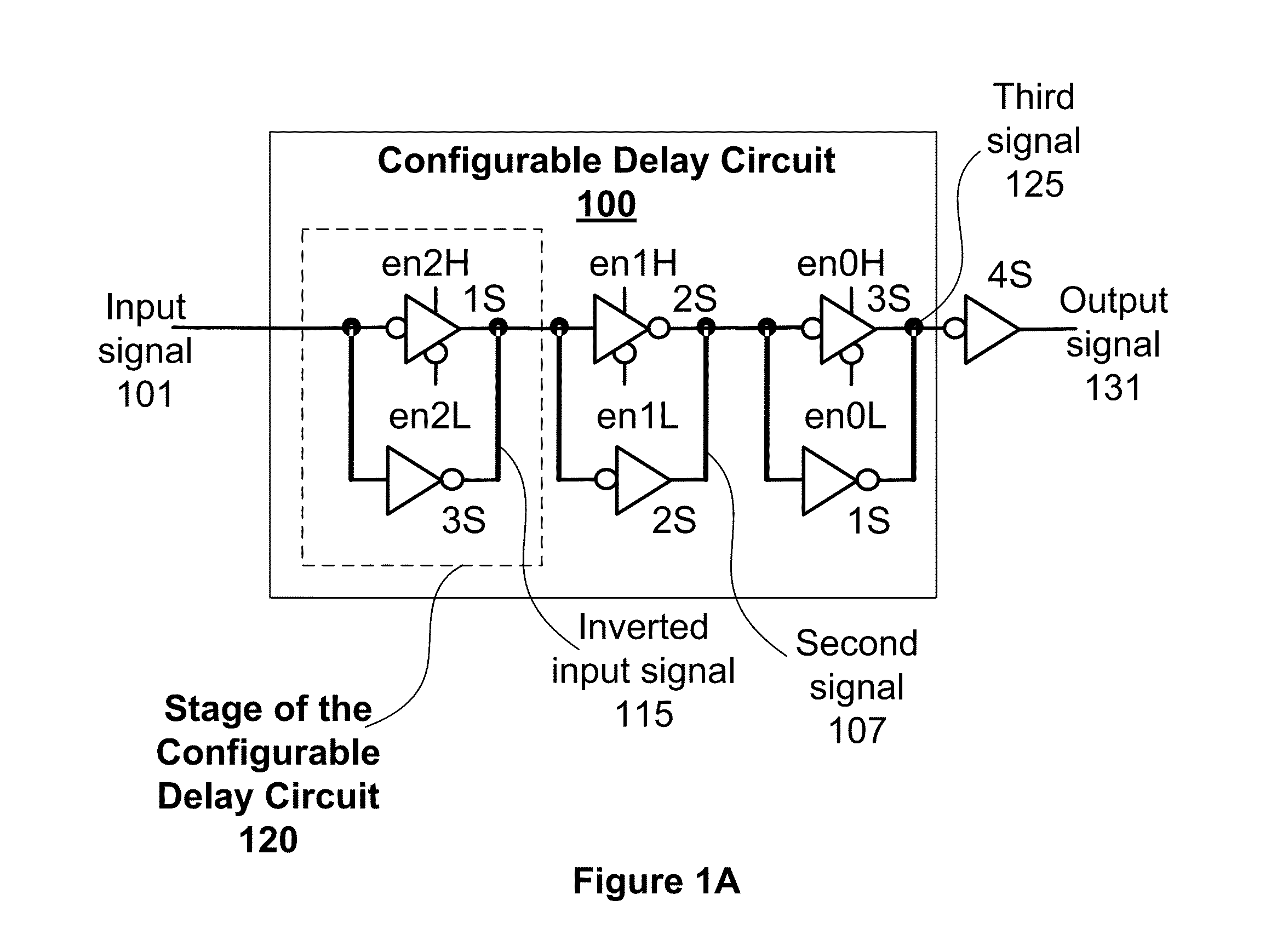
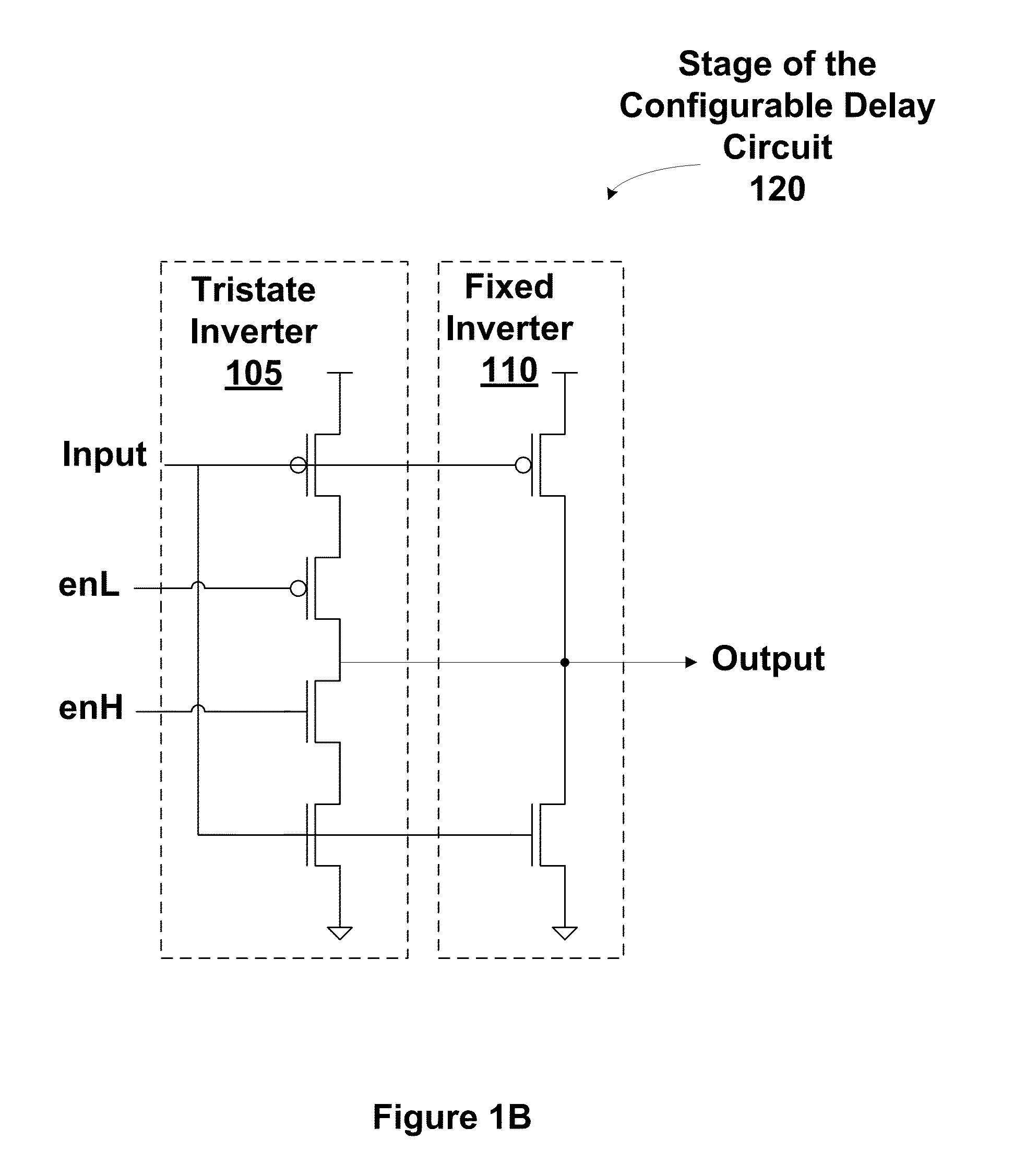
[0033]A configurable delay circuit can be used to correct mismatches in delays between signals such as between clock signals and data and between different bits of data within a multi-bit data bus. Misaligned clock edges relative to data signals can result in functional errors, e.g., timing errors. The configurable delay circuit may be used to align the clock relative to the data signals and ensure that timing requirements are better met.

[0034]Mismatches in delays between different signals of a multi-bit data bus present challenges for meeting the timing requirements to correctly sample...


PUM


Abstract

One embodiment sets forth a timing calibration technique for on-chip source-synchronous, complementary metal-oxide-semiconductor (CMOS) repeater-based interconnect. Two transition patterns may be applied to calibrate the delay of an on-chip data or clock wire. Calibration logic is configured to apply the transition patterns and then trim the delays of the clock and data wires based on captured calibration patterns. The trimming adjusts the delay of the clock and data wires using a configurable delay circuit. Timing errors may be caused by crosstalk, power-supply-induced jitter (PSIJ), or wire delay variation due to transistor and wire metallization mismatch. Chip yields may be improved by reducing the occurrence of timing errors due to mismatched delays between different wires of an on-chip interconnect.

Description

BACKGROUND OF THE INVENTION[0001]1. Field of the Invention[0002]The present invention generally relates to timing calibration and, more specifically, to timing calibration for on-chip interconnect.[0003]2. Description of the Related Art[0004]A source-synchronous, complementary metal-oxide-semiconductor (CMOS)-repeater-based interconnect provides a simple, high-performance topology for global on-chip communication fabrics. However as silicon die sizes increase, the on-chip interconnect may span 10 mm or more in length, and the communication channels are subject to many sources of timing error, including crosstalk, power-supply-induced jitter (PSIJ), and wire delay variation, due to transistor and wire metallization mismatch.[0005]For a 10-mm lower-level metal wire with 130 um width and space, 50% utilization on adjacent layers, and with repeater size and optimized for the minimum power-delay product, the 1-σ delay variation is about 8 ps per transition polarity per wire due to transi...

Claims


Application Information

Patent Timeline
IPC IPC(8): H03H11/26H01L23/52
CPCH03K5/131H03K5/133H01L2924/0002H01L2924/00
Inventor PALMER, ROBERTPOULTON, JOHN W.GREER, III, THOMAS HASTINGSDALLY, WILLIAM JAMES
Owner NVIDIA CORP
Learn More