
Semiconductor nanocrystals used with LED sources

Active Publication Date: 2012-07-12
NANJING TECH CORP LTD +1
View PDF10 Cites 55 Cited by
  • Summary
  • Abstract
  • Description
  • Claims
  • Application Information

AI Technical Summary

Benefits of technology

[0019]The present invention includes several advantages, not all of which are incorporated in a single embodiment.
[0020]Semiconductor nanocrystals, as band-gap absorbers, demonstrate very high absorbances with no back-scattering, as these are less than 10 nm in size, and can use a single excitation frequency wherein multiple colors can be mixed in any proportion to yield high performance lighting without adverse temperature sensitivity. In turn, this provides tremendous LED design flexibility as well as the ability to use LEDs with emission frequencies wherein the intrinsic efficiency of the LEDs is highest.
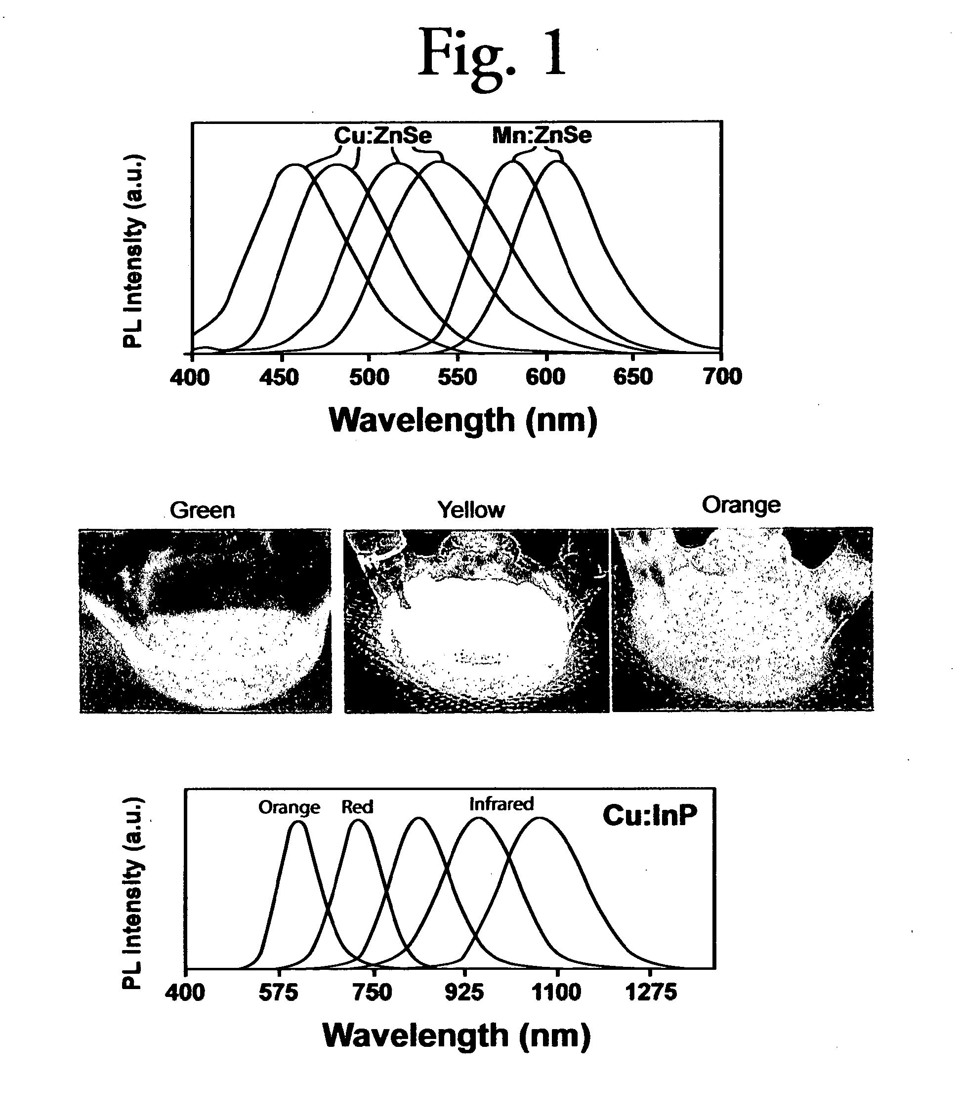
[0021]In comparison to other down-conversion luminescence materials, including rare earth based phosphors and intrinsic quantum dots, the semiconductor nanocrystals according to the present invention possess several unique and outstanding advantages for solid state lighting, abbreviated herein as SSL, applications, such as high photoluminescence (PL) quantum yield (QY>85%), continuously tunable emission peak position, very good thermal stability in both color and intensity, high absorption cross-section, zero scattering, and zero self-quenching. These properties of the semiconductor nanocrystals utilized in the present invention enable superior lighting performance, greater product design flexibility, simplified manufacturing operations and substantially reduced manufacturing costs.

Problems solved by technology

However, white LEDs often suffer from large variations in brightness due to the manufacturing process.
Binning adds huge cost and complexity to the production operation, requiring an additional expensive step and, more importantly, significantly reducing yield.
Severe binning criteria can lead to the rejection of >90% of the LEDs.
While this method eliminates phosphor conversion losses, this method is viewed as complex and has limited achievable efficacy.
Neither technique addresses the problems of wafer variability resulting in binning.
No. 2010 / 0067229A1 by A. M Scotch et al. of Osram Sylvania describe the problem that certain types of LEDs, coated with a phosphor to generate white light, exhibit variations in color temperature due to differences in raw material sources, crystal growth, handling, storage conditions for the raw materials, and the other variables that go into the manufacturing process.
Such binning processes significantly increase the cost of manufacturing the LEDs.
The problem with this solution is that, in reality, it is challenging to find such ‘smart’ combinations.
In addition, this solution does not help with binning that is required due to variation in peak intensity of emitted light or forward voltage differences.
However, existing rare-earth phosphors are insufficient to achieve high performance warm white light.
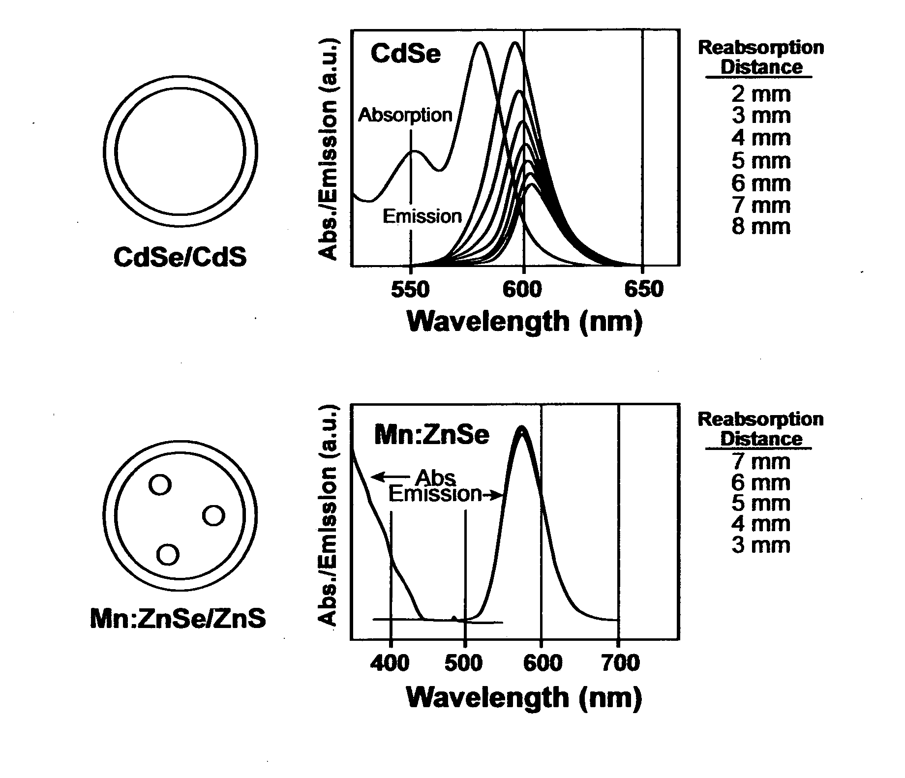
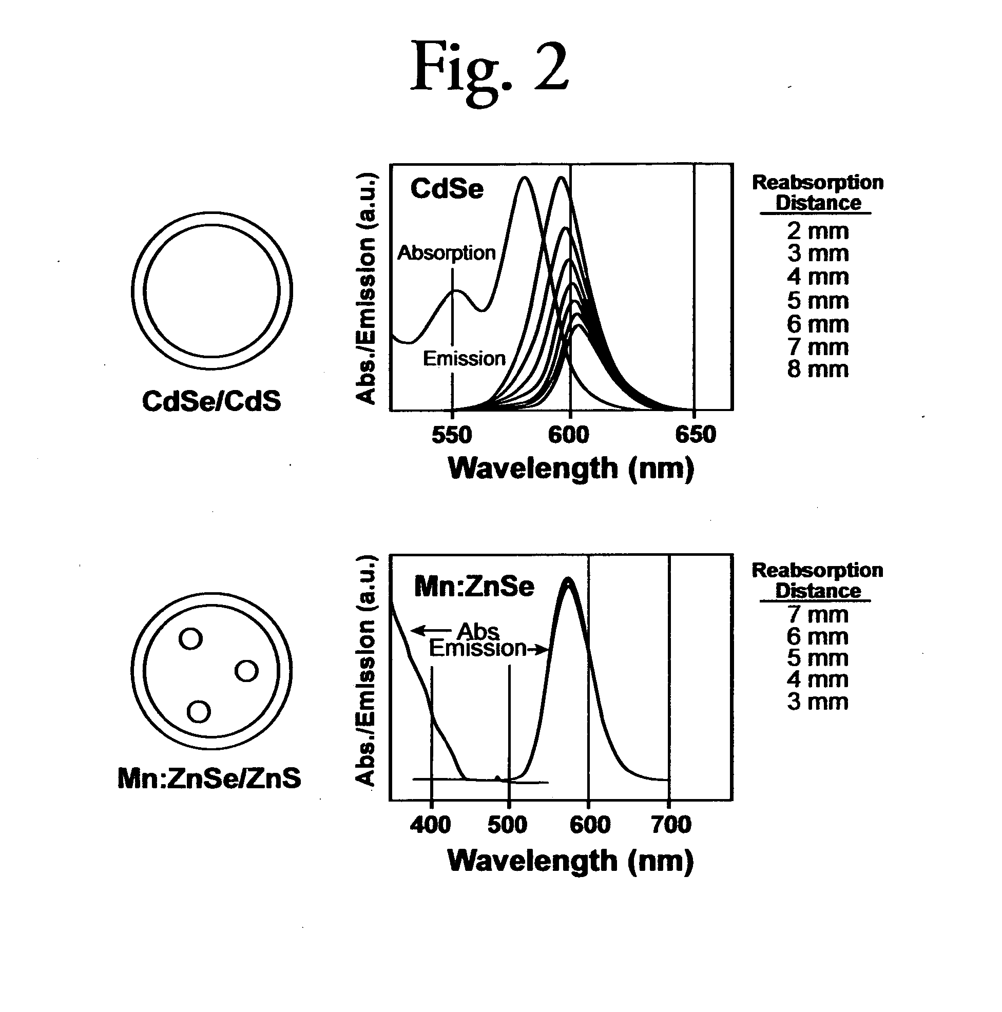
Rare-earth phosphors induce back-scattering, with losses as high as 60%, and are difficult to mix as different colors have different excitation wavelengths and different temperature sensitivity / degradation characteristics.
While this solution is effective, it is simply prohibitive in complexity and cost for most applications, and particularly for applications such as general illumination lighting which are highly cost sensitive.

Method used


Image

  • Semiconductor nanocrystals used with LED sources
  • Semiconductor nanocrystals used with LED sources
  • Semiconductor nanocrystals used with LED sources

Examples


example 1

Synthesis of Cu Doped ZnSe Quantum Dots

Chemicals Used:

[0093]Zinc acetate, 1-Octadecene (ODE), Oleylamine (70%), Decanoic Acid (99+%), Tributylphosphine (TBP) were purchased from Aldrich, and Copper Chloride 99.999% (anhydrous), Manganese Chloride (99+%), Zinc Chloride (99+%), and Oleic Acid from Alpha Aesar. Se and S powder were also purchased from Aldrich. Manganese Stearate was purchased from City Chemical.

Preparation of Zinc Oleate:

[0094]Zinc Chloride (ZnCl2), anhydrous—-6.841 g

[0095]Oleic Acid—28.241 g

[0096]Tetramethyammonium Hydroxide (TMAH)—18.123 g

Molar Ratios: 2:2:1 Oleic Acid:TMAH:ZnCl2, respectively.

Synthesis Procedure Used

[0097]1. Dissolve the ZnCl2 in 200 mL of methanol in a 250 mL separatory funnel.

[0098]2. Dissolve the Oleic Acid and TMAH in 500 mL methanol in a 1 L 3-neck round bottom flask. Stir 30 minutes at room temperature.

[0099]3. Add the ZnCl2 drop wise to the stirring solution of Oleic Acid and TMAH over a period of 1-2 hours.

[0100]4. Allow the reaction to stir...

example 2

Synthesis of Mn Doped ZnSe Quantum Dots

Synthesis Procedure of Mn Doped ZnSe Quantum Dots:

[0140]1. Place a stir bar into a clean, dry 250 mL three-neck round bottom flask.

[0141]2. To the 250 mL 3-neck round bottom flask, add 0.2 g Manganese Stearate and 50 g ODE.

[0142]3. Place the flask in a fitted heating mantle. Attach a condenser, thermocouple sleeve, and septum. Turn on an Argon flow through the flask.

[0143]4. Bubble Argon through the solution while stirring.

[0144]5. Heat the reaction solution up to 120° C. while bubbling Argon for at least 15 minutes.

[0145]6. The Zinc injection solution, growth solution, and amine solution are best effective when heated to 100° C. and purged with Argon before use. For the Zinc injection solution it will need to be heated to at least 100° C. before injection.

[0146]7. Heat the reaction solution up to 270° C., the reaction may be a slight brownish color but will be completely clear at 270° C. If the reaction does not become clear or is very dark / co...

example 3

Dispersion of Doped Quantum Dots in Polymer (Silicone)

[0161]A specific amount of solution (either Hexanes or Chloroform) containing a concentrated amounts of purified d-dots is added to an amount of Dow Corning 2-8630 silicone polymer fluid. Typically, 100 mg of d-dots are added to 5 grams of 2-8630 silicone fluid. The amounts will depend upon use, but maximum concentrations are 250 mg of d-dots in 1 gram of 2-8630 silicone fluid. The fluid mixture is then shaken / stirred vigorously until the nanomaterials are fully dissolved. The fluid is then put under vacuum for 12-24 hours to remove all excess solvent. The silicone fluid is then removed from the vacuum chamber and 250 μL of chloroform containing 150 μg of trimethylolpropane triacrylate (TMPTA) is added. 50 μL of chloroform and 30 μg of TMPTA are needed to cure 1 gram of 2-8630 silicone fluid. Chloroform is necessary to uniformly distribute the TMPTA curing agent throughout the 2-8630 silicone fluid. The mixture is then shaken / sti...


PUM


Abstract

The present invention relates to the use of light-converting, colloidal, doped semiconductor nanocrystals to provide a new generation of high performance, low cost monochromatic and white light sources based on LEDs.

Description

CROSS REFERENCE TO RELATED APPLICATIONS[0001]Priority is claimed to:U.S. Provisional Patent Application Ser. No. 61 / 269,909 by T. Qiao et al., entitled “DOPED SEMICONDUCTOR NANOCRYSTALS USED WITH LED SOURCES”, filed on Jun. 30, 2009, the disclosure of which is incorporated herein by reference.FIELD OF THE INVENTION[0002]The present invention relates to the use of light-converting, colloidal, semiconductor nanocrystals to provide a new generation of high performance, low cost monochromatic and white light sources based on light emitting diodes, also referred to herein by the abbreviation LEDs.BACKGROUND OF THE INVENTION[0003]Solid-state lighting for general illumination, particularly white LEDs, is being viewed by many as a means of meeting the world's growing needs for lighting, while reducing the associated energy costs. However, white LEDs often suffer from large variations in brightness due to the manufacturing process. Thus, the lighting community has asked the light emitting di...

Claims


Application Information

Patent Timeline
IPC IPC(8): H01L33/06B82Y99/00
CPCC09K11/883Y02B20/181H01L33/502Y02B20/00
Inventor QIAO, TIECHENGBATTAGLIA, DAVIDSUNDERRAJAN, SURESHZHANG, QIANGZHU, HAOGUO
Owner NANJING TECH CORP LTD
Learn More