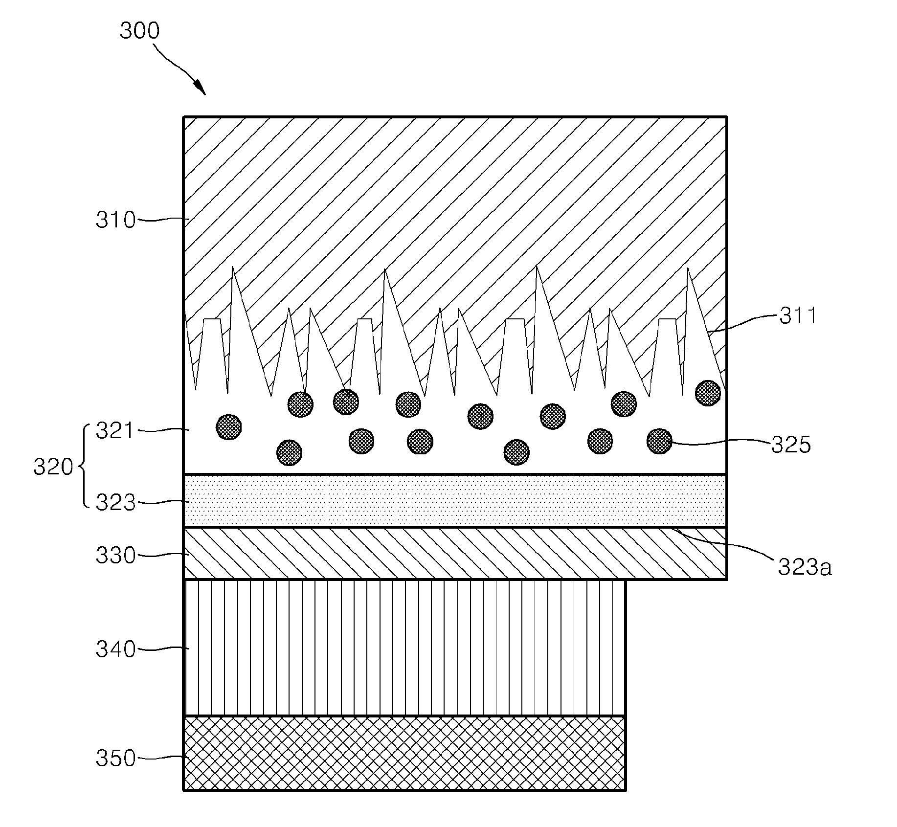
Substrate for surface light emitting device and method of manufacturing the substrate, surface light emitting device, lighting apparatus, and backlight including the same
- Summary
- Abstract
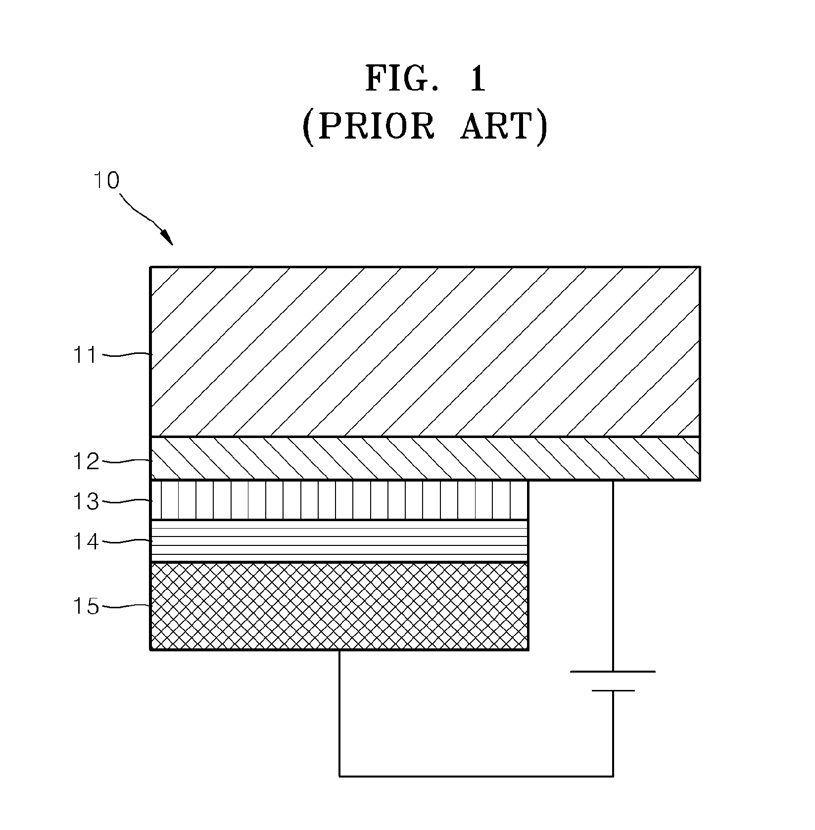
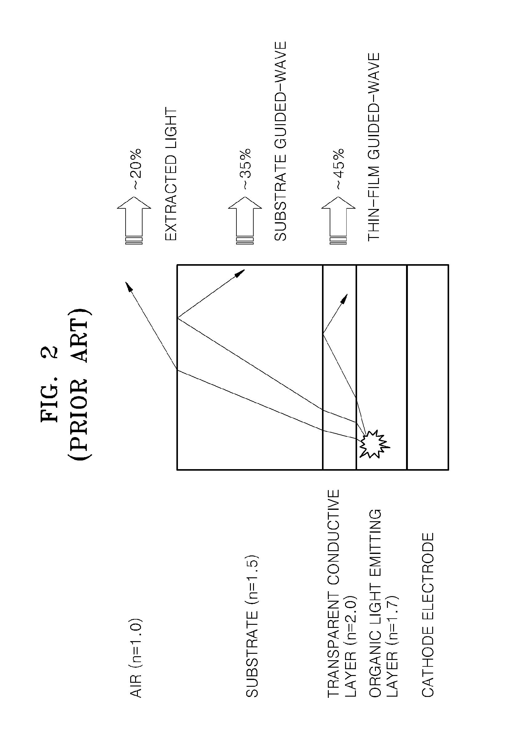
- Description
- Claims
- Application Information
AI Technical Summary
Benefits of technology
Problems solved by technology
Method used
Image

Examples
embodiment
[0229]Hereinafter, the present invention will now be described in more detail with reference to embodiments, but the present invention is not limited thereto.
(Manufacture of the Substrate for Light Emitting Device)
[0230]First, a substrate for a light emitting device used as a substrate of an OLED or the like is manufactured.
[0231]In detail, a support substrate (also referred to as “corrugated substrate”) may be obtained by spraying (sand blast) aluminum powder of #800 at a pressure of about 0.5 kilopascal (kPa) onto a soda lime glass having dimensions of 50 millimeter (mm)×50 millimeter (mm) and a thickness of about 0.7 mm. In such an embodiment, a surface of the corrugated substrate includes ridges having an average surface roughness Ra of about 0.7 μm when observed using a laser microscope (e.g., VK9510, a product of Keyence Co.). In such an embodiment, when the surface of the corrugated substrate was measured using a Hazemeter (e.g., Haze guard II which is a product of Dongyang p...
first embodiment
[0255]To evaluate an OLED having the structure according to the first embodiment of the present invention, substrate samples T1-1 through T1-6 were manufactured as will be described below. Substrate T1-1 is a sample substrate manufactured for comparison and is a glass substrate on which indium tin oxide (ITO) was formed directly as a transparent electrode. Substrate T1-2 was formed by coating a non-corrugated glass substrate with a glass paste composite (nd=1.98, composition: to be described later) having a refractive index that is similar to that of a transparent electrode (ITO) by using a bar coating method, and then sintering the resultant in the air (Air) to form a highly refractive layer thereon. Substrate T1-3 was formed by coating a non-corrugated glass substrate with a glass paste composite (nd=1.98, composition: prepared by dissolving and mixing Bi2O3—B2O3—SiO2—ZnO based glass frit (Tg=400° C.), ethylcellulose STD45 (available by Dow Chemicals), terpineol, and butylcarbitol...
second embodiment
[0259]To evaluate OLED having the structure according to the second embodiment of the present invention, Substrates T2-1 through T2-3 were manufactured. Substrate T2-1 is manufactured for comparison and is a glass substrate on which ITO was directly formed as a transparent electrode. Substrate T2-2 was formed by coating a glass substrate, on which a non-uniform corrugate structure is formed by sand blasting, with a glass paste composite (nd=1.98, composition: prepared by dissolving and mixing Bi2O3—B2O3—SiO2—ZnO based glass frit (Tg=400° C.), ethylcellulose STD45 (available by Dow Chemicals), terpineol, and butylcarbitol acetate) having a refractive index that is similar to that of a transparent electrode (ITO) by using a bar coating method, and then sintering the resultant first in the air (Air), and then the glass paste composite was coated again thereon and then the substrate was sintered in a vacuum (Vac.) to form a highly refractive layer having a two-layer structure thereon. S...
PUM
 Abstract
Description
Claims
Application Information
 - R&D
- Intellectual Property
- Life Sciences
- Materials
- Tech Scout
- Unparalleled Data Quality
- Higher Quality Content
- 60% Fewer Hallucinations
Browse by: Latest US Patents, China's latest patents, Technical Efficacy Thesaurus, Application Domain, Technology Topic, Popular Technical Reports.
© 2025 PatSnap. All rights reserved.Legal|Privacy policy|Modern Slavery Act Transparency Statement|Sitemap|About US| Contact US: help@patsnap.com