
Structure and method for mobility enhanced mosfets with unalloyed silicide

a technology of enhanced mobility and silicide, which is applied in the field of semiconductor devices and manufacturing methods of complementary metal oxide semiconductors (cmos) transistors, can solve the problems of similar problems encountered with silicon substitutional alloys, the general complexity of such processes remains a challenge, and the successful implementation of pfets and nfets with enhanced mobility through stress engineering on the same silicon substrate requires a complex integration of processing steps

Active Publication Date: 2012-06-14
AURIGA INNOVATIONS INC
View PDF2 Cites 7 Cited by
  • Summary
  • Abstract
  • Description
  • Claims
  • Application Information

AI Technical Summary

Benefits of technology

The present invention provides methods and structures for creating stable and low contact resistance on SiGe alloy and Si:C alloy surfaces, as well as improving mobility for both types of transistors on the same substrate. The invention addresses the need for a better method of providing a stable silicon layer on the source and drain regions of transistors, as well as a way to enhance the performance of both types of transistors on the same substrate. The invention also provides a way to deposit a thick epitaxial silicon layer on an insulator substrate, which can be useful in some cases. Overall, the invention provides a solution for creating high-quality semiconductor structures with improved performance and stability.

Problems solved by technology

Similar problems are encountered with substitutional alloys of silicon and germanium.
While the second approach does produce devices with improved performance, such an approach faces some challenges in that the formation of a crystalline structure with an altered lattice parameter generally depends on the structural relaxation of the epitaxially grown alloy material, be it an alloy of silicon and germanium or an alloy of silicon and carbon, through the generation of misfit dislocations, which are crystalline defects in thick films.
Manufacturing both PFETs and NFETs with enhanced mobility through stress engineering on the same substrate, therefore, creates a challenge in that two types of substrate areas with an altered lattice parameter need to be fabricated.
However, the general complexity of such processes still remains a challenge.
As in the case of the second approach discussed above, a successful implementation of both PFETs and NFETs with enhanced mobility through stress engineering on the same silicon substrate requires a complex integration of processing steps.
The first problem is a degradation of contact resistance on SiGe alloy.
As the content of germanium increases, the contact resistance to the source and drain also tends to increase and degrade the performance of PFETs with embedded SiGe alloy in the source and the drain.
This is because the alloy of metal silicide and metal germanide, which is formed by depositing a metal on the source and drain containing silicon and germanium and annealing the structure during the contact formation process, has inferior contact resistance to unalloyed metal silicide, that is, a metal silicide without any metal germanide mixed within.
Metal silicides formed upon such surfaces have degraded performance compared to normal silicide formed on flat surface containing no carbon.
Furthermore, it has been discovered that not only the reaction rate of the Si:C selective epitaxy process is very slow, but there is also a limit on the thickness of the Si:C films that can be grown by selective epitaxy process currently available in the industry.
This means that the increase in the height of the source and the drain through the use of Si:C selective epitaxy has a limit, and that Si:C selective epitaxy is not conducive to manufacturing of NFET structures with highly raised source and drain relative to the height of the gate dielectric.

Method used


Image

  • Structure and method for mobility enhanced mosfets with unalloyed silicide
  • Structure and method for mobility enhanced mosfets with unalloyed silicide
  • Structure and method for mobility enhanced mosfets with unalloyed silicide

Examples


first embodiment

[0051]The present invention has twelve embodiments. Despite the high number of embodiments, however, all of these embodiments share common processes and features. Therefore, the present invention is described in detail for the Thereafter, the differences among the different embodiments of the preset invention are compared and described.

[0052]In typical CMOS processing, some areas of the surface of the semiconductor substrate are used for building PFET structures. These areas are collectively called “the PFET area” herein. Similarly, some other areas of the surface of the semiconductor substrate are used for building NFET structures. They are collectively called “the NFET area herein”. An exemplary PFET structure in the PFET area and an exemplary NFET structure in the NFET area at various stages of the manufacturing sequences are described for the description of the present invention herein.

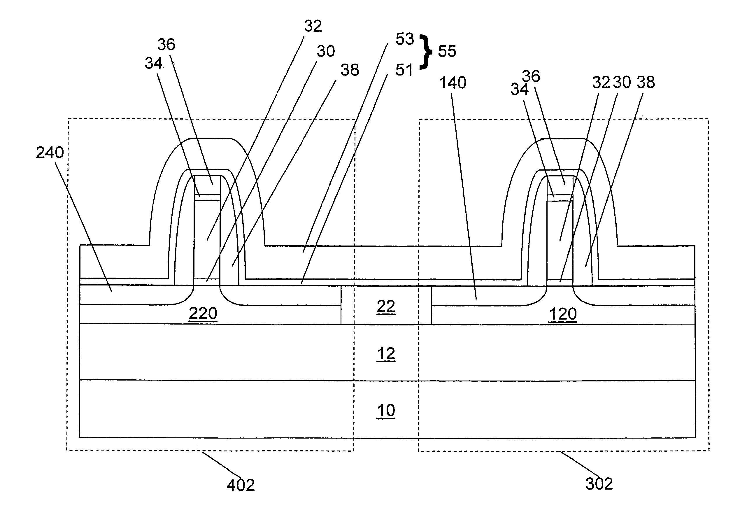
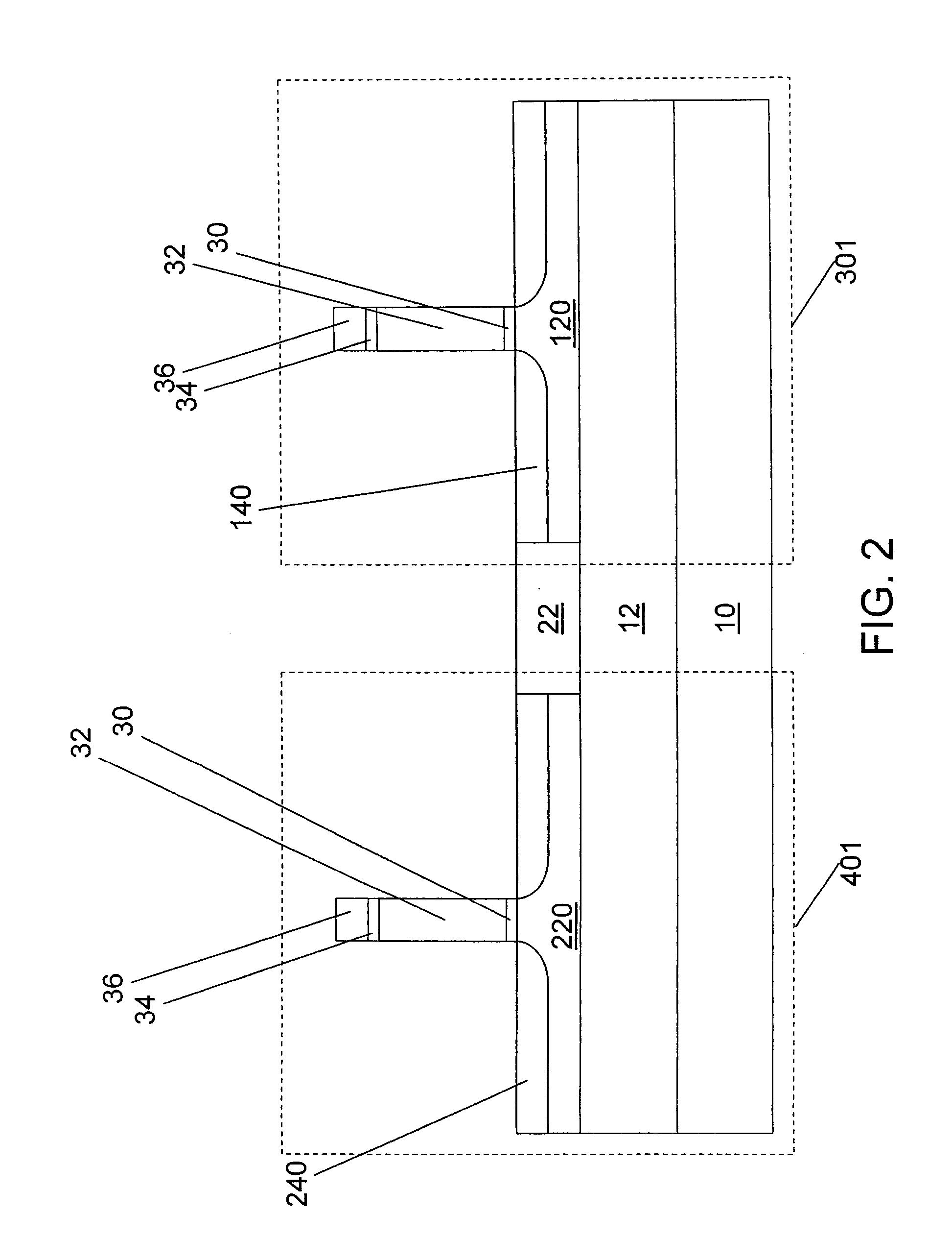
[0053]Referring to FIGS. 2-12, the structures according to the first embodiment of the presen...

seventh embodiment

[0090]According to the present invention, the reaction of the metal 80 is controlled such that the contact formation process consumes only a portion of the N-doped Si:C alloy layer 872′ and the P-doped silicon layer. A PFET structure 711 and an NFET structure 811 at this stage is shown in FIG. 20. The body of the PFET 120, the PFET extension 144, the P-doped silicon 762, the P-doped silicon germanium alloy 762′, and the unreacted P-doped silicon layer 772 form a contiguous single crystalline structure within each area surrounded by STI 22. Likewise, the body of the NFET 220, the NFET extension 244, the N-doped silicon 862, the N-doped Si:C alloy 862′, and the unreacted N-doped silicon layer 874′ form a contiguous single crystalline structure within each area surrounded by STI 22.

[0091]According to the eighth embodiment of the present invention, the reaction of the metal 80 is controlled such that the contact formation process consumes all of the N-doped Si:C alloy layer 872′ and the...

tenth embodiment

[0094]As shown in FIG. 22, a PFET structure 908 is covered with a sixth photoresist 975 and carbon is implanted into the NFET structure 1008. This introduces carbon into the epitaxially grown silicon layer as well as into the silicon material from the substrate. The sixth photoresist 975 is then removed and the silicon substrate is subjected to an anneal process. The SPE during the anneal process produces Si:C alloy 1060′ and an Si:C layer 1070′ in the NFET structure 1008. The lack of doping in the Si:C layer 1070′ in the ninth and tenth embodiment is a new feature not found in prior embodiments. Resist 975 is removed after the SPE.

[0095]Electrical doping of the source and drain regions of the PFETs and NFETs is performed thereafter. FIG. 23 shows the resulting structures. A PFET structure 909 now contains P-doped silicon 762, P-doped silicon germanium alloy 762′, and P-doped silicon layer 772. An NFET structure 1009 contains N-doped silicon 1062, N-doped Si:C alloy 1062′, and N-dop...


PUM

PropertyMeasurementUnit
temperatureaaaaaaaaaa
lattice constantsaaaaaaaaaa

Abstract

While embedded silicon germanium alloy and silicon carbon alloy provide many useful applications, especially for enhancing the mobility of MOSFETs through stress engineering, formation of alloyed silicide on these surfaces degrades device performance. The present invention provides structures and methods for providing unalloyed silicide on such silicon alloy surfaces placed on semiconductor substrates. This enables the formation of low resistance contacts for both mobility enhanced PFETs with embedded SiGe and mobility enhanced NFETs with embedded Si:C on the same semiconductor substrate. Furthermore, this invention provides methods for thick epitaxial silicon alloy, especially thick epitaxial Si:C alloy, above the level of the gate dielectric to increase the stress on the channel on the transistor devices.

Description

CROSS REFERENCE TO RELATED APPLICATION[0001]This application is a divisional of U.S. patent application Ser. No. 11 / 619,809, filed Jan. 4, 2007 the entire content and disclosure of which is incorporated herein by reference.FIELD OF THE INVENTION[0002]The present invention relates to semiconductor devices and methods of manufacture, and particularly, to complementary metal oxide semiconductor (CMOS) transistors with stress in the channels.BACKGROUND OF THE INVENTION[0003]Each new generation of semiconductor technology demands higher performance in semiconductor devices, particularly in the performance of CMOS transistors. One of the key metrics of transistor performance is the on-current of the transistor per unit width, typically measured in hundreds of microamperes per micron of the channel width, or “gate width” as it is commonly referred to. Various methods have been considered and practiced to enhance the on-current of the CMOS transistors, that is, both PFETs (transistors where...

Claims


Application Information

Patent Timeline
Patent Type & Authority Applications(United States)
IPC IPC(8): H01L21/8238
CPCH01L21/823807H01L21/823814H01L21/823864H01L21/84H01L27/1203H01L29/165H01L27/3279H01L29/6656H01L29/66628H01L29/66636H01L29/7848H01L21/76886H01L29/665H01L21/8238H10K59/1315
Inventor LIU, YAOCHENGCHIDAMBARRAO, DURESETIGLUSCHENKOV, OLEGHOLT, JUDSON R.MO, RENEE T.RIM, KERN
Owner AURIGA INNOVATIONS INC
Learn More