
Solid State Supercapacitor and Method for Manufacturing the Same

a supercapacitor and solid-state technology, applied in the field of solid-state supercapacitor, can solve the problems of reducing the permittivity of ceramic materials, reducing the purity of materials and permittivity, and limiting the length and width of mlcc, etc., to achieve high densification, high permittivity, and high purity

Inactive Publication Date: 2012-05-24
DELIJIOU IND & SYST
View PDF0 Cites 3 Cited by
  • Summary
  • Abstract
  • Description
  • Claims
  • Application Information

AI Technical Summary

Benefits of technology

[0012]The present invention relates to a solid state supercapacitor and a method for manufacturing the same so that an objective of high energy capacity and high energy density is reached.
[0017]Compared with a capacitor in prior art, the solid state supercapacitor of the present invention has characteristics of high power density and high energy density. The withstand voltage value is adjustable by the width of the space between two nanowire bundle electrodes. Therefore, the solid state supercapacitor of the present invention is applicable to DC power storages of various voltages and AC power equipments.

Problems solved by technology

Although a ceramic capacitor has high permittivity, its permittivity can be further enhanced, there is still a lot deficiencies due to its manufacturing conditions: first, the ceramic material needs to go under a crushing process after calcination, which may cause pollution and decrease the permittivity of the ceramic material; second, binding agents are added into the ceramic material for molding, which lowers the purity of the material and permittivity; third, after sintering, the ceramic material has a smooth surface so it can only be combined with a plane electrode or other electrodes which does not have large surface area, such as a disc capacitor or an MLCC.
In terms of MLCC, at present the length and the width of an MLCC are limited for production.
At present, a capacitor manufactured by conventional methods can not have characteristics of large surface area and super high permittivity both, and thus a capacitor having super large unit volume of capacity cannot be manufactured.
For instance, although an electrolytic capacitor and an electric double-layer supercapacitor are both conductors having large surface area, the utility of an electrolytic solution prevents a dielectric layer of high permittivity, high durability, high security, and high withstand voltage value, and the working temperature is also limited.
When the polarity is opposite or the voltage is excessive, the insulation layer is damaged and causing a leakage of electricity; further, the electrolytic solution is decomposed and gas is therefore generated; as a result, security problems such as blow-ups of capacitors and systems explosion are caused.
Although electric double-layer capacitors have large surface area for conducting, the utility of aqueous electrolyte in cells results in disadvantages of very low withstand voltage value, very low permittivity, slow response speed, maximum voltage less than 3V, and serial connections are needed to obtain higher voltages, which additionally costs configurations of power management system and causes danger of operation.
However, the disadvantages of the prior art lie in: since a thin-film processing is performed, the stress of a mixed slurry is difficult to eliminate.
It is also difficult to overcome problems such as the generation of impurities, micro cracks and bubbles.
Even if a ceramic glass substrate material is utilized as a matrix, it still indirectly lowers the effective permittivity, generates problems of thermal shocks, impurities, mechanical stresses, etc., and causes problems of internal cracks of the dielectric material.
Furthermore, since maximum voltage is not high enough due to the thin-film processing and should be obtained by serial connections, if one layer in the serial connections structure is an open circuit or a short circuit, the entire energy storage unit will fail or the maximum voltage is lowered, which causes security problems.
Meanwhile, it is noted that a high purity of composition-modified barium titanate material is utilized and a sintering process of thin-film processing the material is performed in order to increase the entire charge storage capacity; however, although this method increases energy density of the energy storage unit, the maximum energy density cannot be really achieved and the production risk cannot be decreased.
It will be very challenging to overcome these defects so this prior art increases costs greatly.
However, if the floating electrode having large surface area is not connected to the external electrode, it is just an image electrode and cannot attract polarized electrical charge; that is this method cannot really manufacture a capacitor with high capacity.
Also, the polymer is very sensitive to the environmental temperature, which will also affect the densification of the material and the distances of the electrodes; as a result, the temperature rises and the entire module expands, the capacity decreases largely and the energy storage is affected.
Furthermore, the floating electrode is too dispersive to control, which easily causes short circuits and therefore is a challenge in manufacturing.

Method used


Image

  • Solid State Supercapacitor and Method for Manufacturing the Same
  • Solid State Supercapacitor and Method for Manufacturing the Same
  • Solid State Supercapacitor and Method for Manufacturing the Same

Examples


Embodiment Construction

[0034]The present invention relates to a solid state supercapacitor, and more particularly to a solid state supercapacitor with a high-purity dielectric material having its highest permittivity, which is done by increasing the surface area of the electrode via nanowire bundles and has the high-purity dielectric material by directly performing a reactive deposition. In the following description, numerous details are set forth in order to provide a thorough understanding of the present invention. It will be appreciated by one skilled in the art that variations of these specific details are possible while still achieving the results of the present invention. In other instance, well-known components are not described in detail in order not to unnecessarily obscure the present invention.

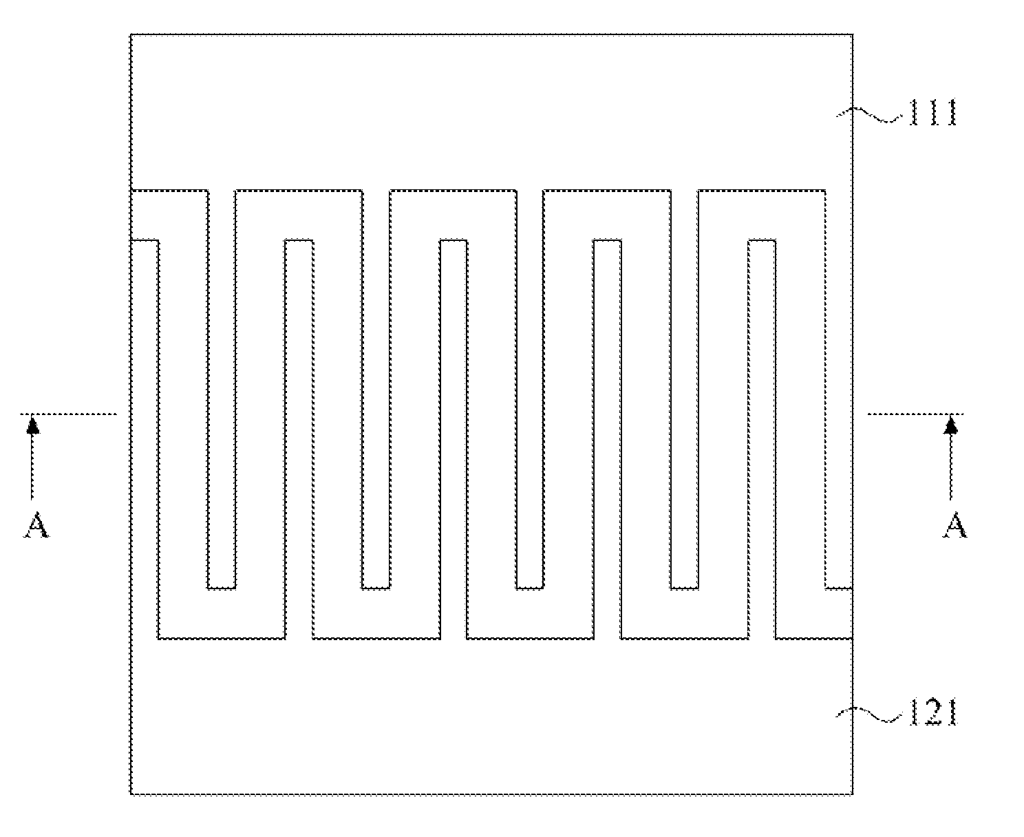
[0035]Referring to FIG. 1, FIG. 1 is a stereogram showing a solid state supercapacitor according to an embodiment of the present invention. The solid state supercapacitor includes a first nanowire bundle ...


PUM

PropertyMeasurementUnit
Densityaaaaaaaaaa
Surface areaaaaaaaaaaa
Energyaaaaaaaaaa

Abstract

A solid state supercapacitor and a method for manufacturing the same is provided, the solid state supercapacitor including two nanowire electrodes with their surface full of nanowire bundle and a dielectric material filled in a space between the two nanowire bundle electrodes and the nanowire bundle, wherein the nanowire bundle includes many nanowires to increase the surface area of electrodes; since the two nanowire bundle electrodes include the nanowire bundle, the surface area thereof is large; a dielectric layer is the original material of the dielectric material, directly reacted, deposited and cured in the space between the two nanowire bundle electrodes without causing pollutions due to additional processing; therefore, the dielectric layer is of high purity and density and has high permittivity to achieve the greatest permittivity of the dielectric material. As a result, the energy capacity of unit volume of the capacitor is effectively increased.

Description

[0001]This application claims the benefits of the Taiwan Patent Application Serial NO. 099139919 filed on Nov. 19, 2010, the subject matter of which is incorporated herein by reference.BACKGROUND OF THE INVENTION[0002]1. Field of the Invention[0003]The present invention relates to a solid state supercapacitor, and more particularly to a solid state supercapacitor with a high-purity dielectric material having its highest permittivity, which is done by increasing the surface area of the electrode via nanowire bundles and has the high-purity dielectric material by directly performing a reactive deposition.[0004]2. Description of the Prior Art[0005]A capacitor is an electrical component for storing energy and is utilized for coupling, flitering, tuning, phase-shifting, storing energy, bypassing, etc. Due to the evolution of high frequency power electronics circuits, high energy density has become the trend of development. Although a ceramic capacitor has high permittivity, its permittiv...

Claims


Application Information

Patent Timeline
IPC IPC(8): H01G9/155H01G13/00B05D5/12B82Y30/00B82Y40/00B82Y99/00
CPCH01G4/005B82Y10/00H01G4/06Y02E60/13
Inventor LIN, TING-KENGGONG, HSIN-GUOCHANG, HUNG-CHINLIN, LI-HUI
Owner DELIJIOU IND & SYST
Learn More