
Plasma doping method and manufacturing method of semiconductor device

a manufacturing method and semiconductor technology, applied in the testing/measurement of individual semiconductor devices, semiconductor/solid-state devices, instruments, etc., can solve the problems of difficult formation of shallow extension regions, inability to achieve uniform in-plane, and inability to achieve uniform deposition of radicals on the surface of the substra

Active Publication Date: 2011-06-02
ULVAC INC
View PDF4 Cites 0 Cited by
  • Summary
  • Abstract
  • Description
  • Claims
  • Application Information

AI Technical Summary

Benefits of technology

The present invention provides a plasma doping method for introducing impurities into an object to be processed, such as a substrate or film, with a uniform distribution. The method involves generating plasma containing the impurities and depositing radicals of the impurities on the surface of the object to be processed. The method also includes radiating ions to the deposited radicals to form an extension region in the object. The plasma doping method separates the steps of depositing the radicals and radiating the ions, resulting in a uniform distribution of the radicals and ions on the surface of the object. This method prevents etching of the surface of the object and ensures low resistance of the extension region.

Problems solved by technology

Consequently, it was difficult to form a shallow extension region by the use of the ion implantation method.
However, because the radicals and the ions are different from each other in the existence of electric charges and the like, and because the radicals exist more than the ions in the plasma, the plasma controlled in order to obtain the uniform in-plane distribution on the surface of the substrate does not enable the obtainment of the uniform in-plane distribution of the radicals on the surface of the substrate, and does not enable the uniform deposition of the radicals on the surface of the substrate.
As a result, the plasma doping method described in the patent document 1 has a problem of the impossibleness of the uniform introduction of impurities into the substrate because the method cannot simultaneously secure both of the uniform in-plane distributions of the radicals and the ions on the surface of the substrate.
Moreover, the plasma doping method causes a disadvantage of the etching of the surface of the substrate by the ions because the drawing speed of the ions is generally faster than the depositing speed of the radicals in the processing apparatus executing the plasma doping method described in the patent document 1.

Method used


Image

  • Plasma doping method and manufacturing method of semiconductor device
  • Plasma doping method and manufacturing method of semiconductor device
  • Plasma doping method and manufacturing method of semiconductor device

Examples


first embodiment

[0041]In the following, a plasma doping method of the present invention will be described with reference to the accompanying drawings. In addition, the elements common to in each drawing are denoted by the same marks, and duplicating descriptions are omitted.

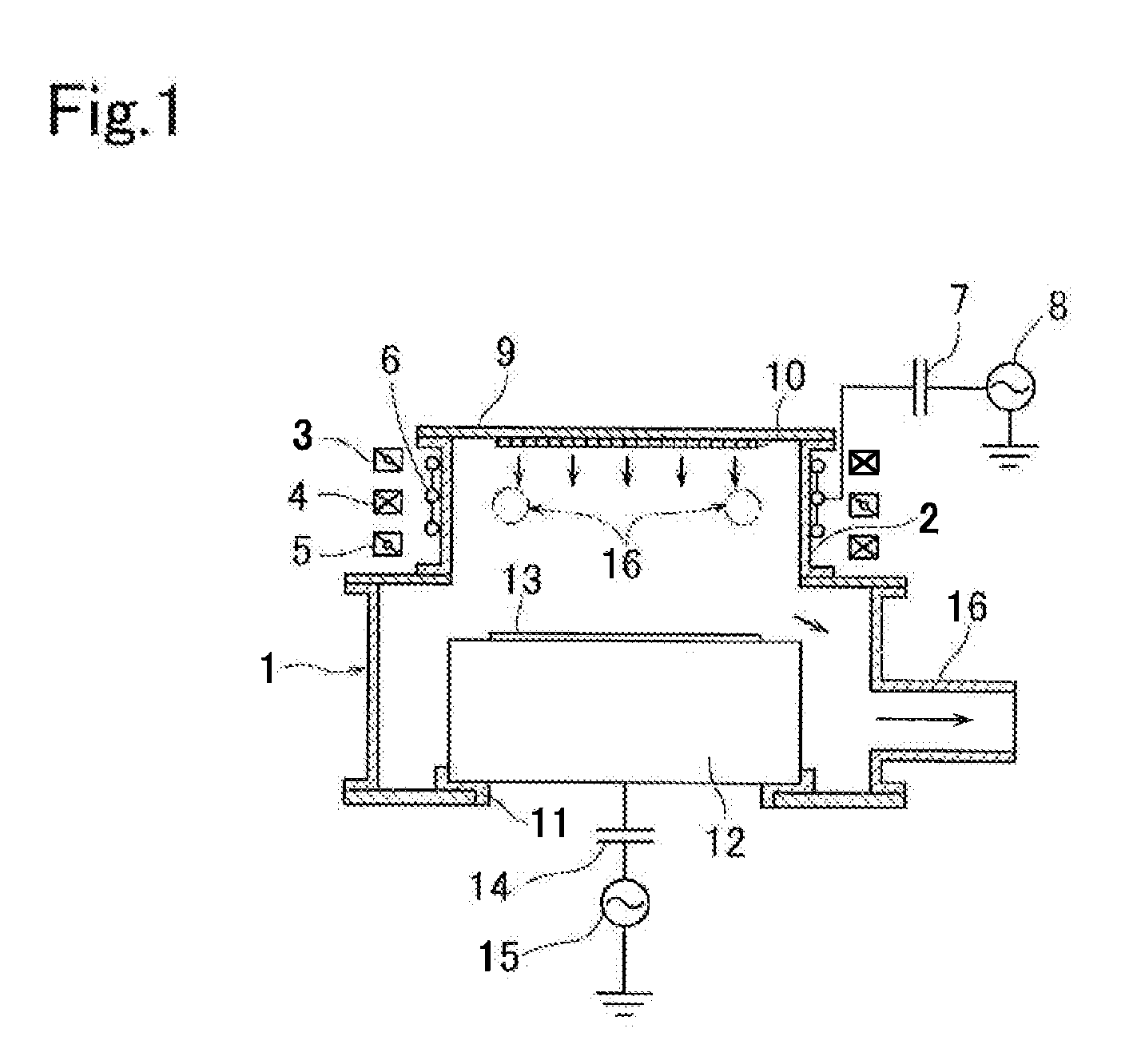
[0042]A processing apparatus used in the present embodiment is, for example, an ICP (inductively coupled plasma) type plasma doping apparatus as shown in FIG. 1, and is equipped with a vacuum chamber 1 capable of forming a vacuum atmosphere.

[0043]The upper part of the vacuum chamber 1 is configured in cylinder portion 2, made of a dielectric, such as quartz, and the cylinder portion 2 functions as a plasma generation unit. Three ring-shaped magnetic field coils 3, 4, and 5, which can form a magnetic neutral line (NLD) in the cylinder portion 2, are arranged on the outside of the cylinder portion 2. A looped antenna coil 6 is arranged between the cylinder portion 2 and the magnetic field coils 3-5. The antenna coil 6 is connected...

second embodiment

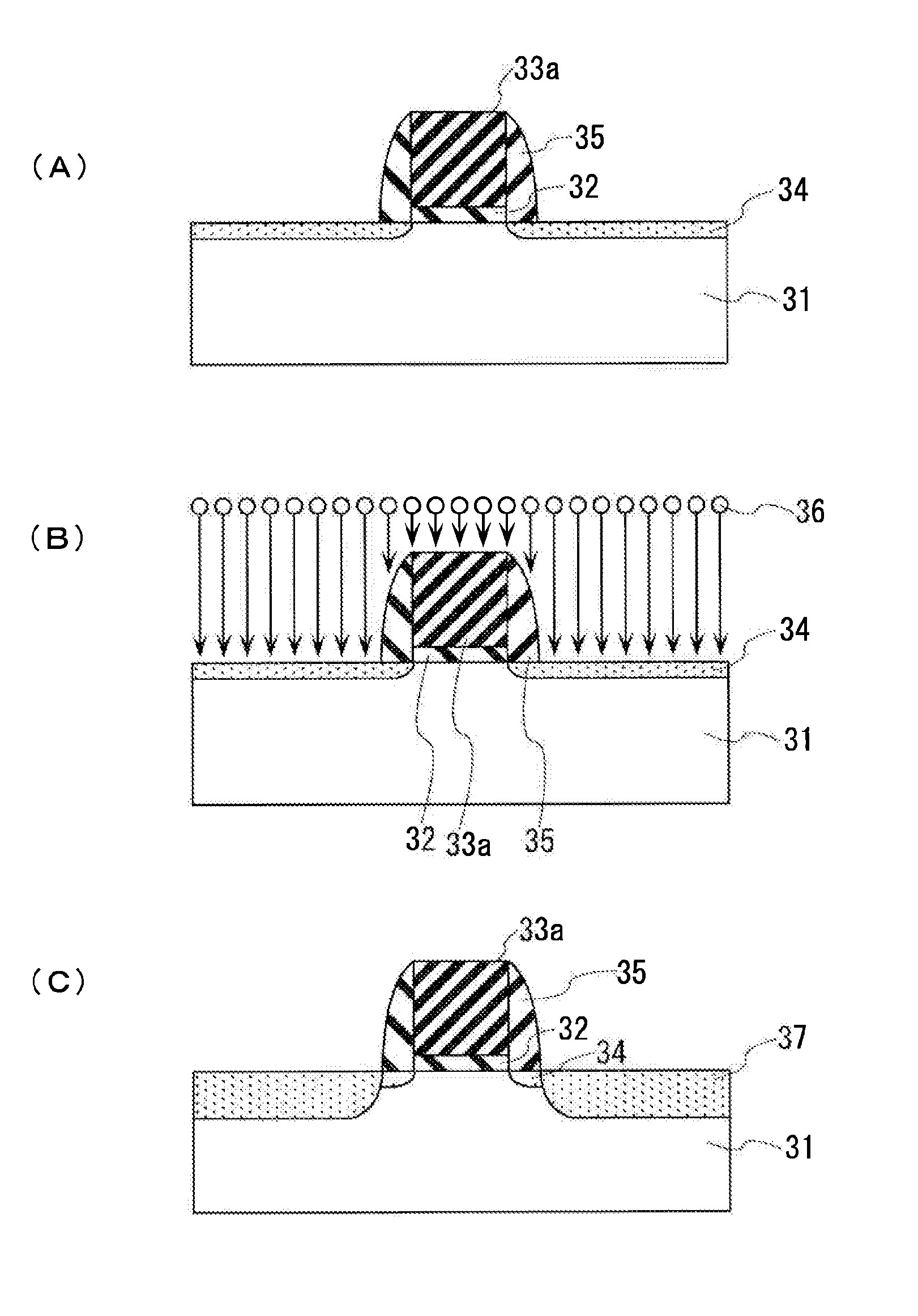
[0101]In the second embodiment described above, after depositing the boron radicals 21 on the surface of the silicon substrate 31, the argon ions 22 are radiated to the deposited boron radicals 21, at the time of forming the extension region 34 after the formation of the gate electrode 33a. The radiated argon ions 22 collide with the boron radicals 21, and thereby the boron radicals 21 are pushed into the silicon substrate 31.

[0102]According to the present embodiment, the deposition step of the boron radicals 21 on the surface of the silicon substrate 31, and the radiation step of the argon ions 22 to the surface of the silicon substrate 31 are separated from each other, the in-plane distribution of the boron radicals 21 and the in-plane distribution of the argon ions 22 on the surface of the silicon substrate 31 can independently be controlled. Consequently, the in-plane distribution of the boron radicals 21 on the surface of the silicon substrate 31 is improved, and rare gas ions ...

third embodiment

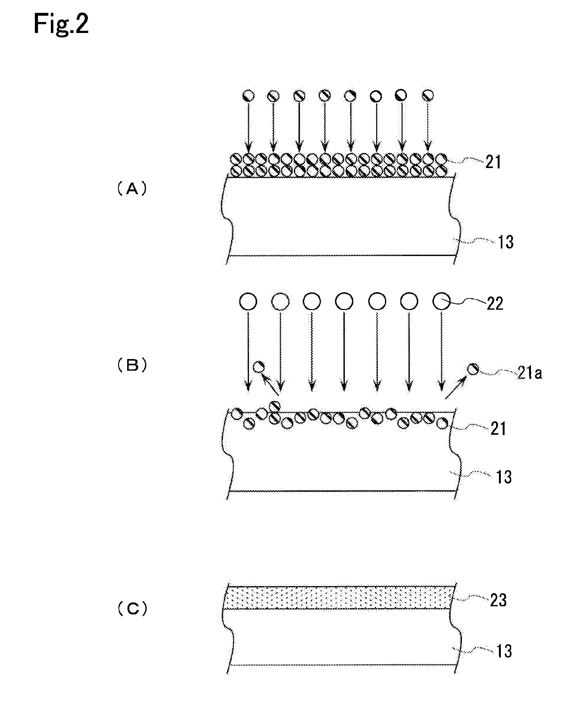
[0121]In the third embodiment described above, while depositing the boron radicals 21 on the surface of the silicon substrate 13, the argon ions 22 drawn into the surface of the silicon substrate 13 are made to collide with the deposited boron radicals 21. Hereby, the boron radicals 21 deposited on the surface of the silicon substrate 13 are pushed into the silicon substrate 13, and a part of the boron radicals 21 is scattered from the surface of the silicon substrate 13.

[0122]According to the present embodiment, the depositing speed of the boron radicals 21 on the surface of the silicon substrate 13 and the etching speed of the boron radicals 21 by the argon ions 22 are made to be equal to each other, and thereby the surface of the silicon substrate 13 is covered by the boron radicals 21 at the time of introducing the boron radicals 21 into the silicon substrate 13. Consequently, the surface of the silicon substrate 13 can be prevented from being etched by the argon ions 22. Conseq...


PUM

PropertyMeasurementUnit
depthaaaaaaaaaa
peak-to-aaaaaaaaaa
thicknessaaaaaaaaaa

Abstract

A plasma doping method capable of introducing impurities into an object to be processed uniformly is supplied. Plasma of a diborane gas containing boron, which is a p-type impurity, and an argon gas, which is a rare gas, is generated, and no bias potential is applied to a silicon substrate. Thereby, the boron radicals in the plasma are deposited on the surface of the silicon substrate. After that, the supply of the diborane gas is stopped, and bias potential is applied to the silicon substrate. Thereby, the argon ions in the plasma are radiated onto the surface of the silicon substrate. The radiated argon ions collide with the boron radicals, and thereby boron radicals are introduced into the silicon substrate. The introduced boron radicals are activated by thermal processing, and thereby a p-type impurity diffusion layer is formed in the silicon substrate.

Description

TECHNICAL FIELD[0001]The present invention relates to a plasma doping method for introducing impurities into the inside of an object to be processed and a manufacturing method of semiconductor device including a formation step of an extension region.BACKGROUND ART[0002]It is known that a short channel effect, in which a leakage current flows at the time of an off-operation of a transistor, arises in an MISFET (Metal Insulator Silicon Field Effect Transistor), which is one of semiconductor devices, when the gate length thereof is short, and it is known to form an extension region which is shallow than the source / drain regions in order to suppress the short channel effect.[0003]In the formation of such an extension region, it is required to form the depth thereof to be more shallow (e.g. 10 nm or less) in association with the recent further miniaturization of the MISFET. The extension region is generally formed by introducing impurities into a substrate, and after that, by activating ...

Claims


Application Information

Patent Timeline
Patent Type & Authority Applications(United States)
IPC IPC(8): H01L21/336H01L21/322
CPCH01L21/2236H01L29/7833H01L29/6659H01L21/02252H01L21/76826H01L21/76856
Inventor TONARI, KAZUHIKONISHIHASHI, TSUTOMU
Owner ULVAC INC
Learn More