Manufacturing apparatus of sic epitaxial wafer and method of manufacturing sic epitaxial wafer
A technology for epitaxial wafers and manufacturing devices, applied in chemical instruments and methods, semiconductor/solid-state device manufacturing, crystal growth, etc., can solve problems such as increased carrier concentration, achieve fluctuation suppression, excellent electrical characteristics, and improve in-plane distribution effect
- Summary
- Abstract
- Description
- Claims
- Application Information
AI Technical Summary
Problems solved by technology
Method used
Image
Examples
no. 1 approach
[0075] Hereinafter, an example of the SiC epitaxial wafer manufacturing apparatus according to the first embodiment of the present invention will be described.
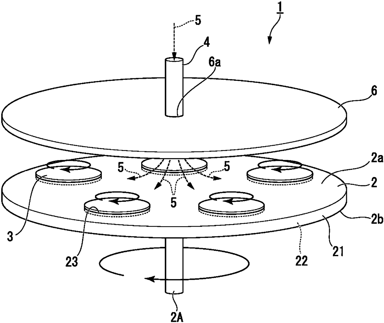
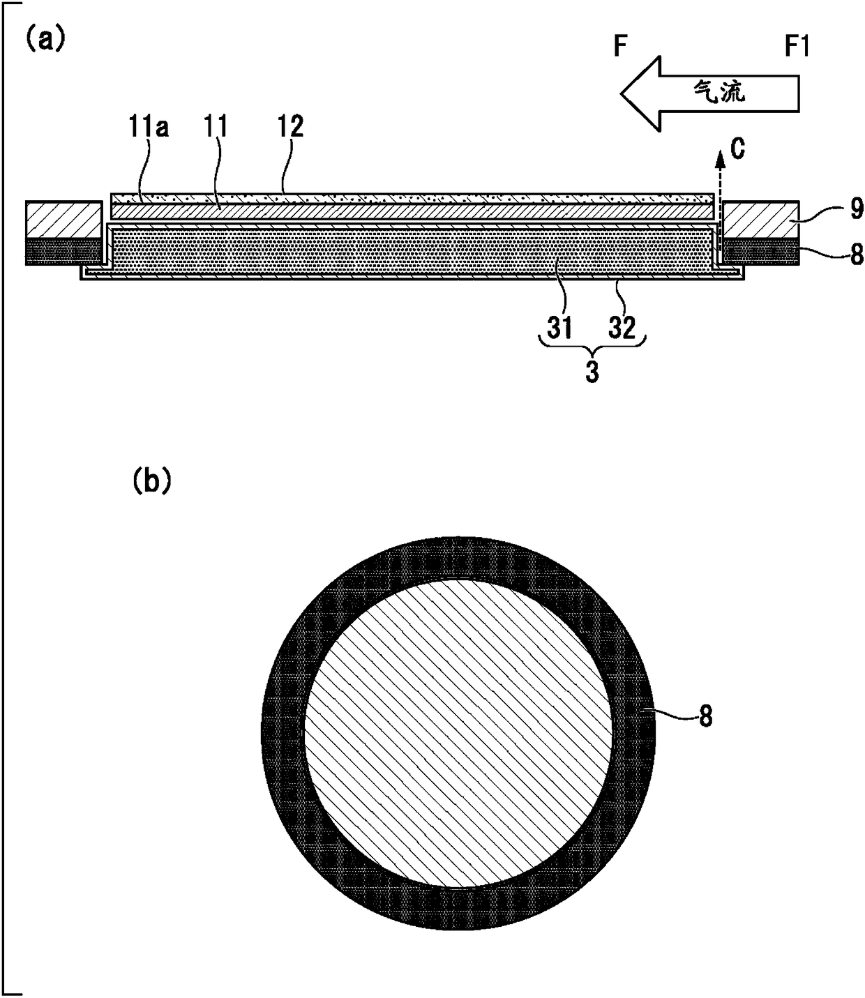
[0076] The manufacturing apparatus 1 of the first embodiment is as figure 1 and figure 2 As shown in (a), the apparatus for growing the SiC epitaxial film 12 on the main surface 11a of the SiC substrate 11 by the chemical vapor deposition method arranges a plurality of wafers (SiC substrates) horizontally as shown in the figure, and rotates each wafer A horizontal rotation-revolving type epitaxial growth device that rotates the wafer itself around the center of the wafer at the same time.
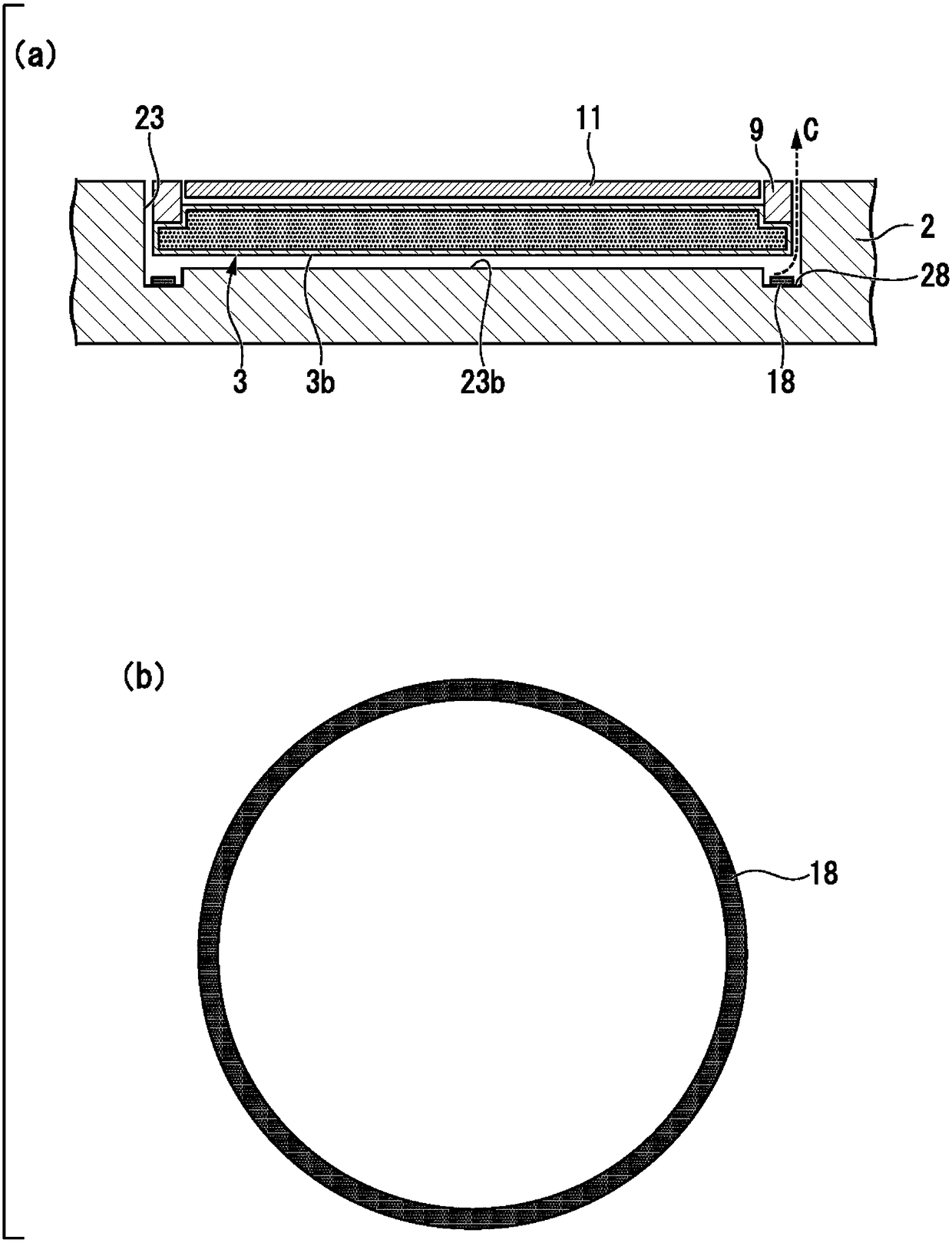
[0077] The SiC epitaxial wafer manufacturing apparatus 1 of the first embodiment is provided with: a concave housing portion 23 (refer to image 3 ) of the loading plate 2; the satellite tray 3 disposed in the concave housing portion 23 on which the SiC substrate 11 can be placed; The carbon member 8 at the position of 11 conta...
no. 2 approach
[0110] The manufacturing apparatus of the second embodiment differs from the manufacturing apparatus 1 of the first embodiment only in the configuration of the satellite disk, and the same configuration as that of the manufacturing apparatus 1 of the first embodiment can be used for other configurations.
[0111] The satellite dish of the second embodiment is composed of a carbon base material coated with a non-carbon material, and has a portion where the carbon base material is exposed at a position not in contact with the placed SiC substrate.
[0112] As an example, such as Figure 4 As shown in (a) and (b), there is a spot facing portion 132a formed in the center of the upper surface 103a of the satellite dish 103 so as not to be in contact with the SiC substrate 11, and the spot facing portion 132a is arranged so as to surround it. In the supporting portion 133 supporting the SiC substrate 11 , at least a part of the bottom surface of the spot facing portion 132 a exposes...
no. 3 approach
[0122] The difference between the manufacturing apparatus of the third embodiment and the manufacturing apparatus 1 of the first embodiment is that the carbon supply source is not arranged near the satellite dish, but is arranged on the upstream side of the raw material gas, that is, between the gas inlet and the satellite dish. between. For other configurations, the same configuration as that of the manufacturing apparatus 1 of the first embodiment can be used.
[0123] The manufacturing apparatus according to the third embodiment includes: a loading plate 202 having a concave storage portion; a satellite plate 203 arranged in the concave storage portion on which the SiC substrate 11 can be placed; The source gas introduction pipe 204 for supplying the source gas 5 of the SiC epitaxial film 12 on the main surface 11a of the SiC epitaxial film 11; side carbon member 208 .
[0124] Figure 6 It is a schematic diagram which shows an example of the manufacturing apparatus of 3...
PUM
 Abstract
Description
Claims
Application Information
 - Generate Ideas
- Intellectual Property
- Life Sciences
- Materials
- Tech Scout
- Unparalleled Data Quality
- Higher Quality Content
- 60% Fewer Hallucinations
Browse by: Latest US Patents, China's latest patents, Technical Efficacy Thesaurus, Application Domain, Technology Topic, Popular Technical Reports.
© 2025 PatSnap. All rights reserved.Legal|Privacy policy|Modern Slavery Act Transparency Statement|Sitemap|About US| Contact US: help@patsnap.com


