
Metal compound, material for chemical vapor phase growth, and process for forming metal-containing thin film

a technology of metal compound and chemical vapor phase, which is applied in the direction of organic chemistry, coatings, liquid/solution decomposition chemical coatings, etc., can solve the problems of poor thermal stability, difficult for the resulting film to exhibit electrical characteristics, and high temperature unsuitable for semiconductor device elements such as gate films, etc., to achieve stable film composition control, reduce residual carbon, and reduce the effect of residual carbon

Active Publication Date: 2010-09-30
ADEKA CORP
View PDF0 Cites 2 Cited by
  • Summary
  • Abstract
  • Description
  • Claims
  • Application Information

AI Technical Summary

Benefits of technology

[0041]The metal compound of the invention affords a metal nitride with little impurity, such as residual carbon, and is therefore preferably used to form a metal nitride thin film. A preferred process for forming a metal nitride thin film using the chemical vapor phase material of the invention is ALD. ALD is a process in which a chemical vapor phase growth material and, if necessary, a reactive gas, and other precursor are alternately pulsed to make one cycle to form an atomic monolayer, and this cycle is repeated until the atomic layers are deposited and built up to a desired thickness. In each cycle, the pulse of the vapor phase growth material and / or the reactive gas may optionally be followed by a step of removing the unreacted vapor phase growth material and / or the unreacted reactive gas by purging with an inert gas and / or by evacuation. ALD is characterized by providing a thin film with a smaller and more uniform thickness than CVD processes. Another advantage of ALD, from the nature of the film formation mechanism, is a lower deposition temperature required. This advantage makes ALD widely applicable independently of the heat resistance of a substrate, diffusivity of the element to a substrate, and the like. ALD may be effected in combination with heat, light, or plasma.
[0059]As shown in Table 2, compound No. 6 of the invention, unlike the analogous compound TiCl2[N(CH3)2]2, is liquid at room temperature and therefore suitable as a material for chemical vapor phase growth. Compound No. 6 was equal to TiCl2[N(CH3)2]2 in thermal decomposability. As compared with compound No. 2, compound No. 6 decomposes at a lower temperature. However, having a decomposition temperature of 100° C. provides a small processing margin. Taking the margin between the volatilization temperature and the film formation temperature into consideration, compound No. 2 is more suitable than compound No. 6 for use in chemical vapor phase growth.Example 3Fabrication of Titanium Nitride Thin Film

Problems solved by technology

However, the film formation process using a chloride typified by titanium tetrachloride needs high temperatures of at least about 500° C. Such a high temperature is unsuitable in the production of a semiconductor device element, such as a gate film.
Although the organic amide metal compound having an organic amine as a ligand is capable of forming a metal nitride thin film at low temperatures, it is difficult for the resulting film to exhibit electrical characteristics as expected because of its high residual carbon content and to be applied to a gate film, a barrier film, or an electrode film that are particularly required to have electrical conductivity.
They, while having good thermal decomposability, have poor thermal stability and can decompose during being heated to be kept in a liquid state for a long period of time.
If used as it is a solid, there arise problems with the material vapor feed and in-line transportation of the material, such as shortage of vapor feed or variation in vapor feed with time.
The problem of contamination with particles also occurs.
Even in a process using a solution, such as a solution CVD process using a solution of a solid precursor in an organic solvent, the solution suffers from precipitation due to change in temperature, partial evaporation of the solvent, and change in concentration in a vaporizer, resulting in clogging of feed piping.
The problem of the feed rate change with time due to, e.g., clogging of feed piping and the problem of contamination with particles remain to be completely settled down.

Method used


Image

  • Metal compound, material for chemical vapor phase growth, and process for forming metal-containing thin film
  • Metal compound, material for chemical vapor phase growth, and process for forming metal-containing thin film
  • Metal compound, material for chemical vapor phase growth, and process for forming metal-containing thin film

Examples


example 1

Preparation of Compound No. 2

[0045]A reaction flask was charged with 43.0 g of titanium tetrachloride (TiCl4) and 500 ml of dehydrated hexane and cooled to −10° C. in a dry argon atmosphere. A mixed solution of 191 g of tetrakis(ethylmethylamino)titanium (Ti[N(CH3)(C2H5)]4) and 500 ml of dehydrated hexane was added thereto dropwise in a manner such that the reaction system temperature might not exceed −5° C. Completion of the dropwise addition was followed by stirring at room temperature for 8 hours. Hexane was removed by evaporation under reduced pressure, and the residue was distilled under reduced pressure. From a fraction collected at a distillation temperature of 82° C. under a pressure of 100 Pa was obtained compound No. 2 in a yield of 90%. Identification of the compound was accomplished by elemental analysis and 1H-NMR analysis. The results of the analyses are shown below.

[0046](1) Elemental analysis (metal analysis via atomic absorption / chloride analysis via silver nitrate ...

example 2

Preparation of compound No. 6

[0051]A reaction flask was charged with 55.7 g of titanium tetrachloride (TiCl4) and 300 ml of dehydrated toluene and cooled to −10° C. in a dry argon atmosphere. A mixed solution of 82.3 g of tetrakis(ethylmethylamino)titanium (Ti[N(CH3)(C2H5)]4) and 300 ml of dehydrated toluene was added thereto dropwise in a manner such that the reaction system temperature might not exceed −5° C. Completion of the dropwise addition was followed by stirring at room temperature for 8 hours. Toluene was removed by evaporation under reduced pressure, and the residue was distilled under reduced pressure. From a fraction collected at a distillation temperature of 85° C. under a pressure of 100 Pa was obtained compound No. 6 in a yield of 90%. Identification of the compound was accomplished by elemental analysis and 1H-NMR analysis. The results of the analyses are shown below.

[0052](1) Elemental analysis (metal analysis via atomic absorption / chloride analysis via silver nitr...

example 3

Fabrication of Titanium Nitride Thin Film

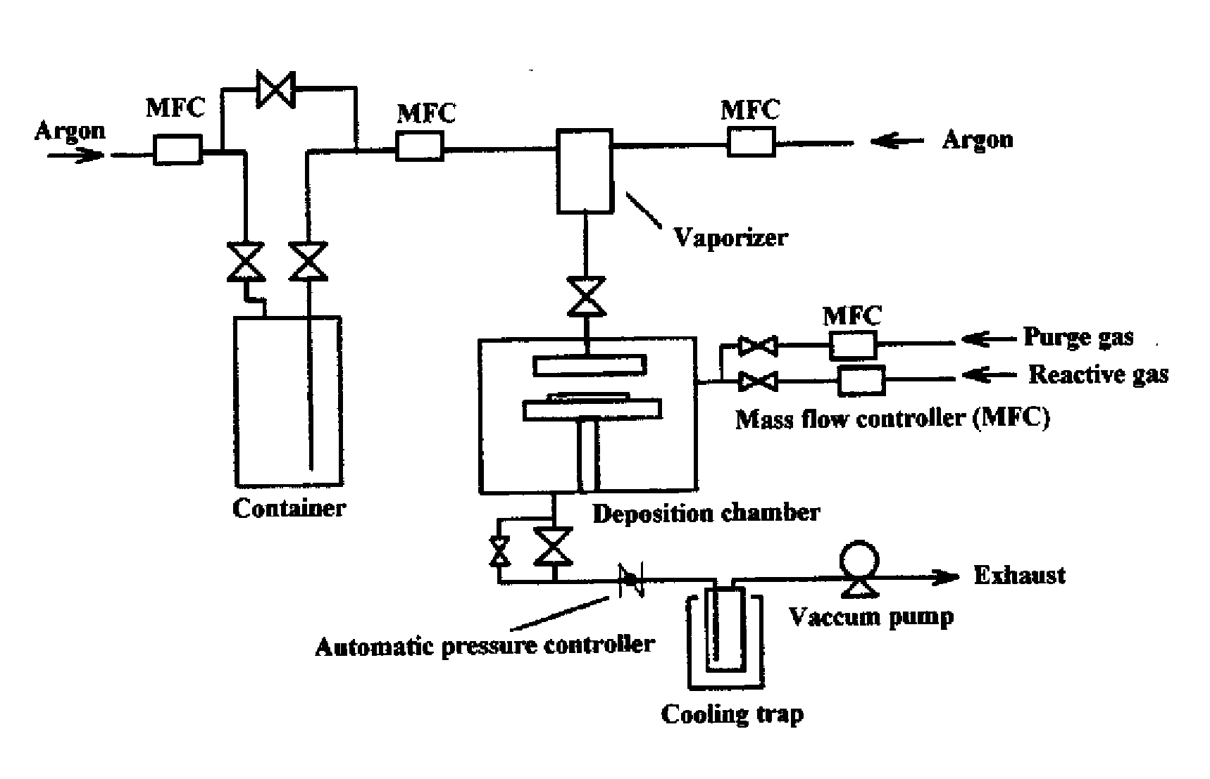
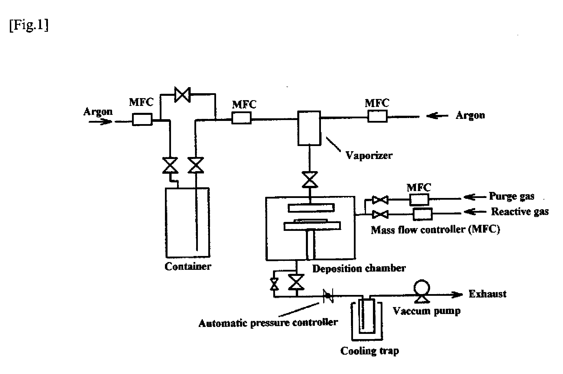
[0060]A titanium nitride thin film was fabricated on a silicon wafer by ALD using the equipment illustrated in FIG. 1 and compound No. 2 obtained in Example 1 as a chemical vapor phase growth material under the conditions described below. The resulting film was analyzed by X-ray fluorometry to determine the film thickness and composition. It was found as a result that the film thickness was 60 nm, the film composition was titanium nitride, and the carbon content was 1.3 at %.

ALD Conditions:

[0061]Reaction temperature (substrate temperature): 300° C.

Reactive gas: NH3

[0062]Three hundred cycles each having steps (1) to (4) were performed.

(1) A CVD material vaporized in the vaporizer at 120° C. and 250 Pa was pulsed into the deposition chamber and allowed to deposit for 3 seconds under a system pressure of 250 Pa.

(2) The chamber was purged with argon for 3 seconds to remove the unreacted material.

(3) The reactive gas was pulsed into the chamber a...


PUM

PropertyMeasurementUnit
temperatureaaaaaaaaaa
melting pointaaaaaaaaaa
pressureaaaaaaaaaa

Abstract

A novel metal compound of general formula (1), a material for chemical vapor phase growth containing the compound, and a process for forming a metal-containing thin film by chemical vapor phase growth using the material. Among the compounds of formula (1), those wherein X is a chlorine atom are preferred because of inexpensiveness and high volatility. When M is titanium, those wherein m is 1 are preferred as having a greater difference between a volatilization temperature (vapor temperature) and a deposition temperature (reaction temperature), which provides a broader process margin.In formula (1), M is titanium, zirconium, or hafnium; X is a halogen atom; and m is 1 or 2.

Description

TECHNICAL FIELD[0001]This invention relates to a novel metal compound having a specific structure, a material for chemical vapor phase growth containing the metal compound, and a process for fabricating a metal-containing thin film using the material.BACKGROUND ART[0002]A thin film containing titanium, zirconium, or hafnium is used as an electronic member of electronic components, such as high dielectric constant capacitors, ferroelectric capacitors, gate films, barrier films, and gate insulators, and an optical element of optical communication devices, such as optical waveguides, optical switches, and optical amplifiers.[0003]Processes for forming the above-described thin film include MOD techniques including a dipping-pyrolysis process and a sol-gel process and chemical vapor-phase growth techniques, such as chemical vapor deposition (hereinafter abbreviated as CVD) and atomic layer deposition (hereinafter abbreviated as ALD). Chemical vapor phase growth techniques involving vapor...

Claims


Application Information

Patent Timeline
Patent Type & Authority Applications(United States)
IPC IPC(8): C23C16/34C23C16/44C07F7/28C07F7/00
CPCC07F7/006C23C16/308C23C16/45553C23C16/40C23C16/34C07F7/003
Inventor YAMADA, NAOKIYOSHINAKA, ATSUYAWADA, SENJI
Owner ADEKA CORP
Learn More