Printable, Flexible and Stretchable Diamond for Thermal Management
- Summary
- Abstract
- Description
- Claims
- Application Information
AI Technical Summary
Benefits of technology
Problems solved by technology
Method used
Image
Examples
example 1
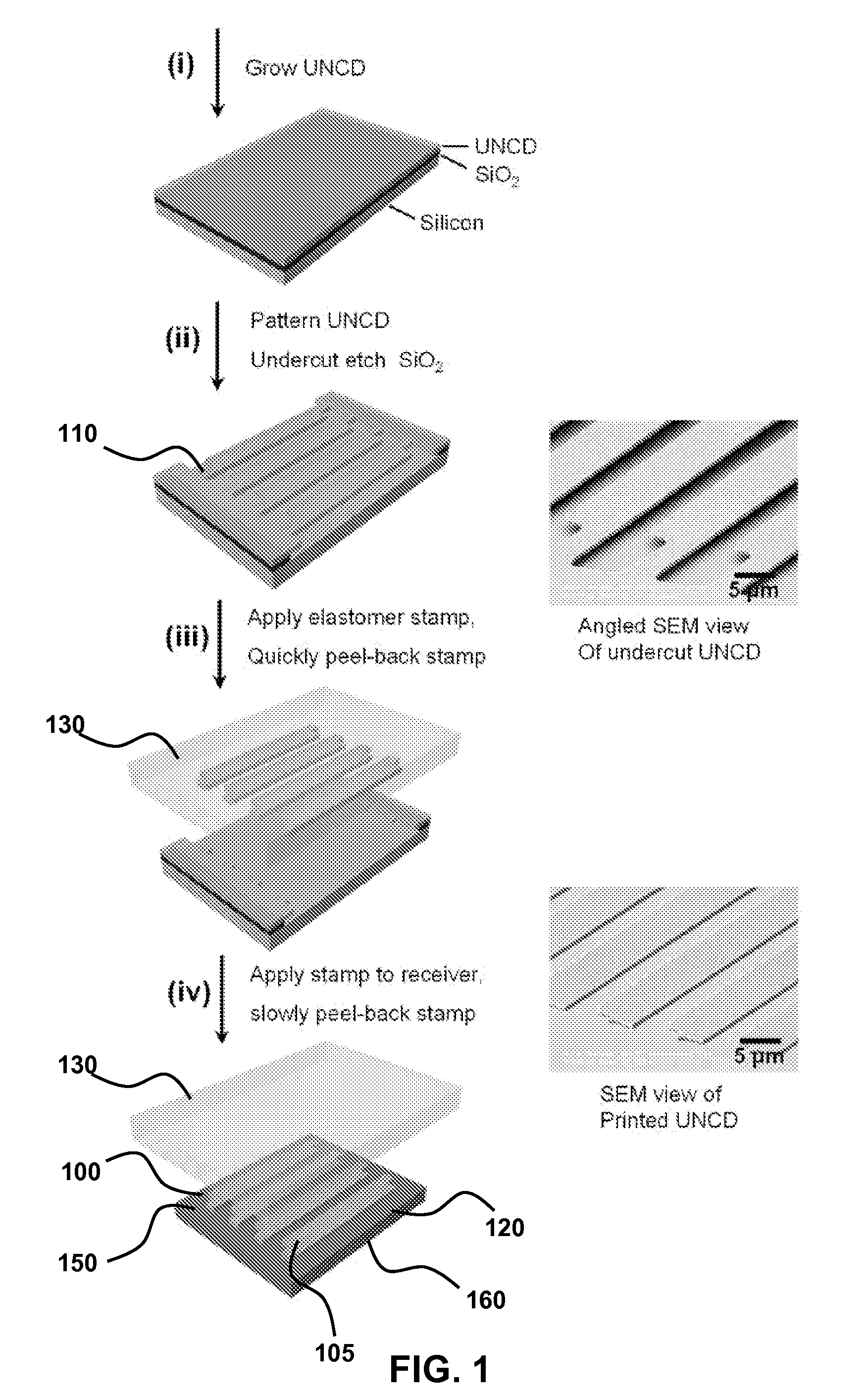
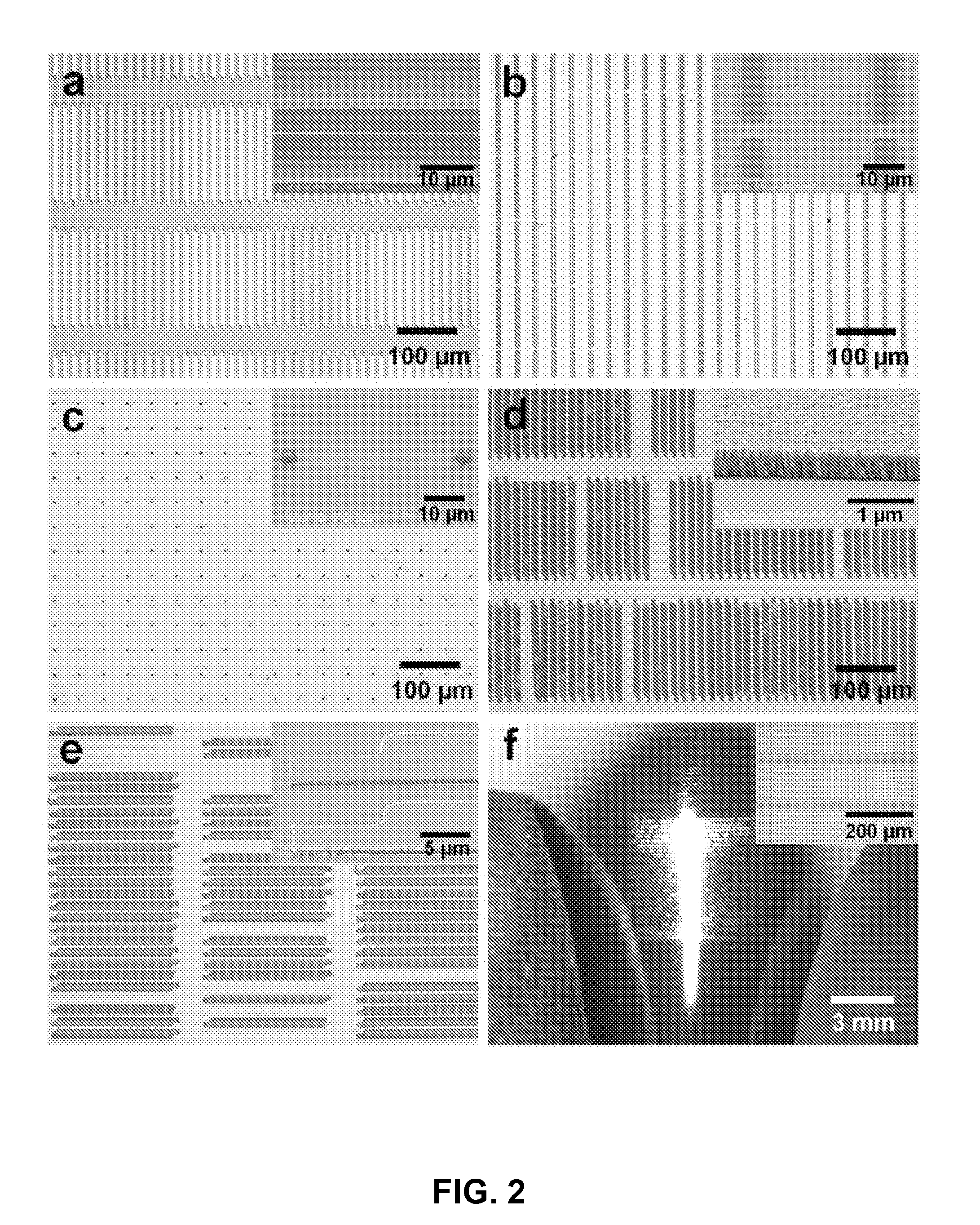
[0078]Thin film diamond has many potential applications in electronics[1] and optoelectronics,[2,3] microelectromechanical systems (MEMS),[4,5] wear resistant coatings[6], thermal management[7] and other areas, due to its exceptional electronic, optical, mechanical, chemical / tribological and thermal properties, respectively.[8-11] Diamond is most commonly implemented in these systems by directly growing the material on the surfaces of device substrates, where it is used as uniform or lithographically patterned films. This approach places restrictions on the range of applications because known growth techniques involve high temperatures, vacuum or low pressure conditions and often other demanding conditions.[12,13] Implementing thin film diamond on low temperature plastics, for example, is not possible. Large area substrates are also not well matched to capabilities of existing deposition techniques, and is particularly cost ineffective when the diamond is only required at sparse cov...
example 2
Efficient Heat Extraction from the Active Junction of Transfer Printed GaN Power HEMTs
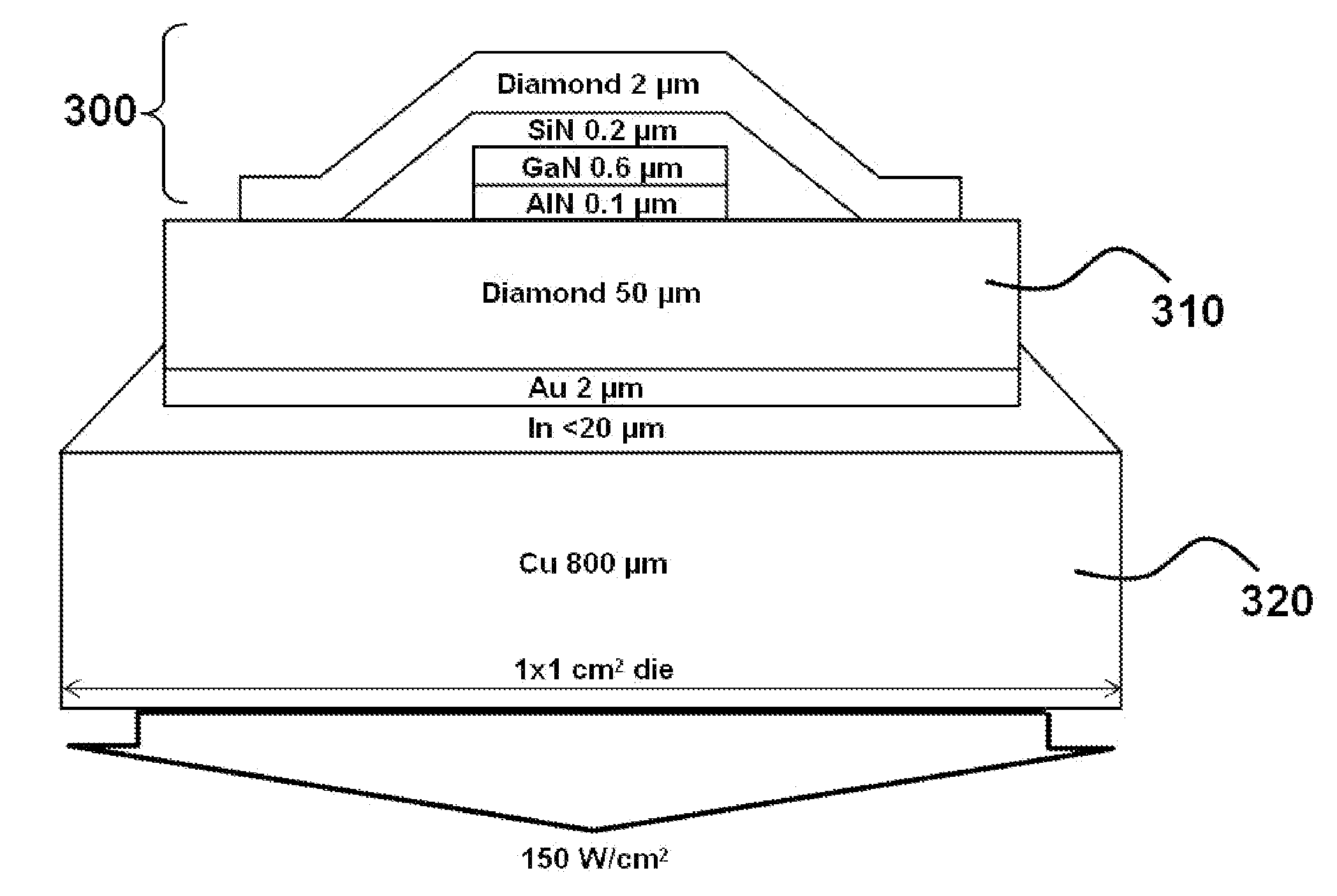
[0125]Excess heat generated by output transistors in high power amplifiers (PA) limit the safe operating area (SOA) and negatively impact surrounding control electronics. Current approaches to substrates for high thermal density include either the integration of functionality on a single semiconductor material as an integrated circuit (e.g., monolithic microwave integrated circuits, MMICs) or the heterogeneous integration of planar layers of varying functional properties (e.g., semiconductor on diamond, SOD). For MMIC devices, integration can be limited by an inability to match semiconductor materials technology with device type. For instance, a high-power GaN PA might be most optimally integrated with a CMOS control circuit for efficient feed-forward digital signal synthesis. Integrated as a single device, the control device can be negatively influenced by thermal losses dissipated from the power ...
example 3
Examples and Analysis of Heat Extraction Devices
[0139]Integration technology achieved via transfer printing can significantly improve overall heat extraction from heat-generating devices, such as from the active junction of GaN high power devices. Exemplary components of such heat-extraction devices include, copper / diamond heat sink substrate, GaN chiplets transfer printed on the heat sink substrate, and thin diamond heat spreaders transfer printed and incorporated into the device. The performance of the semiconductor device platforms are evaluated and compared to conventional state of the art semiconductor platforms.
[0140]A state of the art GaN on SopSiC is illustrated in FIG. 12A. A corresponding semiconductor platform incorporating the processes and systems provided herein for improved heat extraction is illustrated in FIG. 12B. The performance of the semiconductor device platform proposed in FIG. 12B is compared against state of the art GaN devices fabricated on Silicon on poly-...
PUM
| Property | Measurement | Unit |
|---|---|---|
| Thickness | aaaaa | aaaaa |
| Width | aaaaa | aaaaa |
| Temperature | aaaaa | aaaaa |
Abstract
Description
Claims
Application Information
 - R&D
- Intellectual Property
- Life Sciences
- Materials
- Tech Scout
- Unparalleled Data Quality
- Higher Quality Content
- 60% Fewer Hallucinations
Browse by: Latest US Patents, China's latest patents, Technical Efficacy Thesaurus, Application Domain, Technology Topic, Popular Technical Reports.
© 2025 PatSnap. All rights reserved.Legal|Privacy policy|Modern Slavery Act Transparency Statement|Sitemap|About US| Contact US: help@patsnap.com


