
Method of making nitride semiconductor laser, method of making epitaxial wafer, and nitride semiconductor laser

a semiconductor laser and epitaxial wafer technology, applied in the field of making nitride semiconductor lasers, epitaxial wafer making methods, and nitride semiconductor lasers, can solve the problems of large amount of laser oscillation threshold current, increase of non-mission parts in ingan well layers, and increase of indium content, so as to reduce the crystal quality of ingan well layers and reduce the effect of indium content and low emission efficiency

Inactive Publication Date: 2009-10-29
SUMITOMO ELECTRIC IND LTD
View PDF4 Cites 15 Cited by
  • Summary
  • Abstract
  • Description
  • Claims
  • Application Information

AI Technical Summary

Benefits of technology

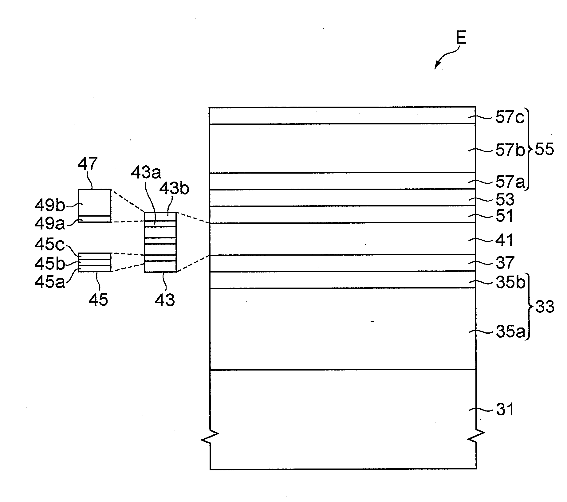
[0009]An InGaN well layer having an indium-rich composition is used to achieve long-wavelength emission in a group III nitride semiconductor laser. The crystal quality of the InGaN well layer is lowered as the indium content is increased. This leads to increase of non-mission part in the InGaN well layer and thus low emission efficiency. Furthermore, such an increase in indium content facilitates a blue shift of the emission wavelength. In a group III nitride semiconductor laser with a large blue shift, the emission wavelength varies with an increase in current which is applied thereto in its LED mode, i.e., before its laser oscillation. Consequently, emission with a blue shift in the LED mode does not contribute to the stimulated emission for laser oscillation. In addition, the increase in indium content in an InGaN well layer broadens the full width at the half maximum of the photoluminescence spectrum. Such a broadened full width at the half maximum enlarges a wavelength band with an optical gain. The emission in the LED mode is generated in a wavelength region in which the emission does not contribute to the laser oscillation, which leads to a large amount of threshold current for laser oscillation.

Problems solved by technology

This leads to increase of non-mission part in the InGaN well layer and thus low emission efficiency.
The emission in the LED mode is generated in a wavelength region in which the emission does not contribute to the laser oscillation, which leads to a large amount of threshold current for laser oscillation.

Method used


Image

  • Method of making nitride semiconductor laser, method of making epitaxial wafer, and nitride semiconductor laser
  • Method of making nitride semiconductor laser, method of making epitaxial wafer, and nitride semiconductor laser
  • Method of making nitride semiconductor laser, method of making epitaxial wafer, and nitride semiconductor laser

Examples


example 1

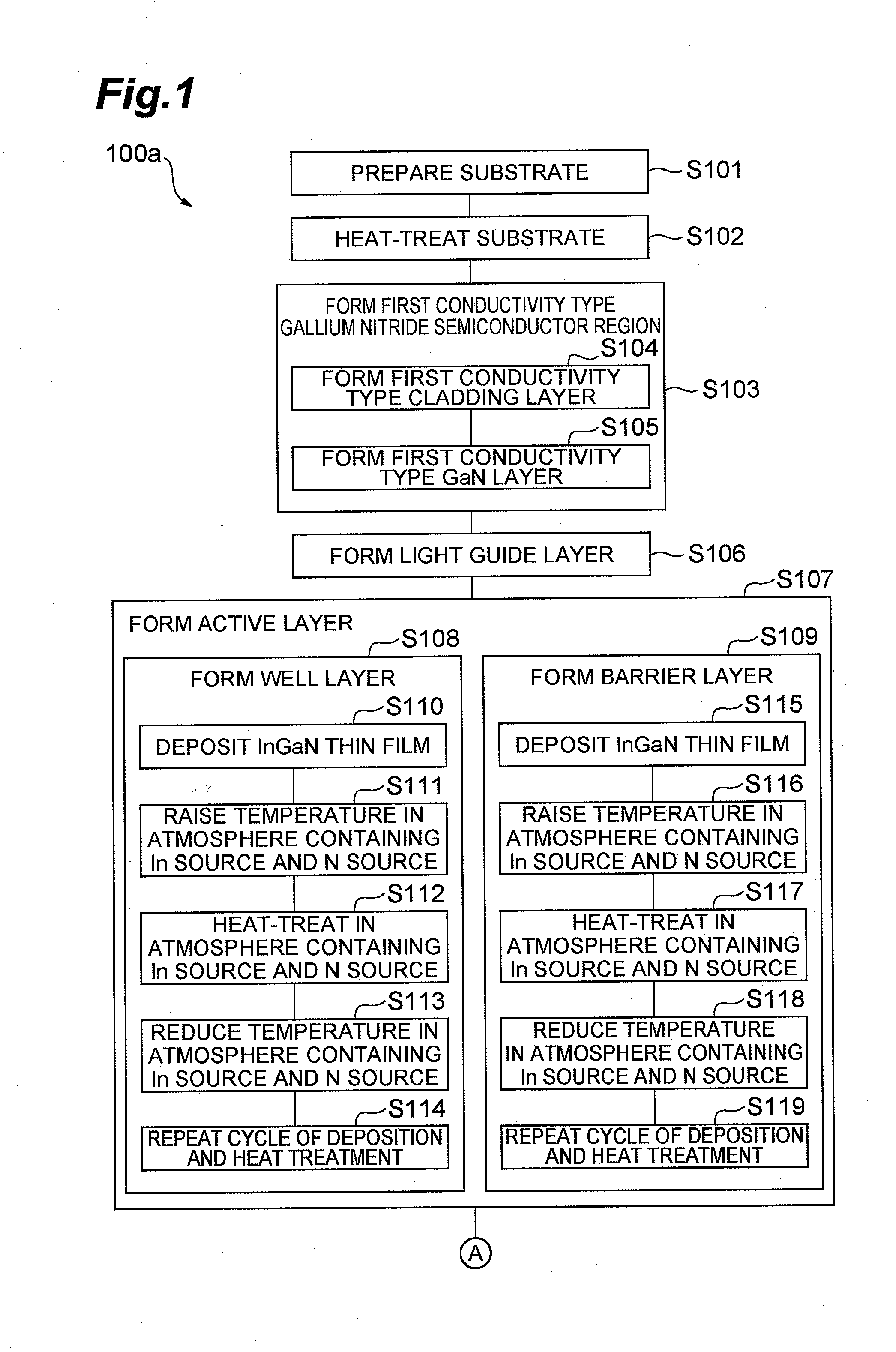
[0089]A group III nitride semiconductor laser was fabricated on the c-plane of a GaN wafer as described in the embodiments above, with the exception of the formation of an active layer. The growth temperature was changed using a resistive heater of a susceptor. FIG. 7 illustrates the primary steps of forming the active layer for the group III nitride semiconductor laser in Example 1. In Step 207, the active layer was formed by the method illustrated in FIG. 7 through organometallic vapor phase epitaxy. After an In0.30Ga0.70N well layer having a thickness of 3 mn was grown at 700° C., in Step 209, an In0.06Ga0.94N barrier layer was grown. First, in Step 210, the In0.06Ga0.94N thin film having a thickness of 1 nm was deposited at 700° C. After the deposition of the thin film, in Step 211, the growth temperature was changed to 850° C. in two minutes, while TMIn and NH3 were supplied to the reactor. In Step 212, the growth temperature remains unchanged at 850° C. for one minute. After k...

example 2

[0091]A group III nitride semiconductor laser was fabricated on the c-plane of a GaN wafer as described in the embodiments above, with the exception of the formation of an active layer. The growth temperature was changed using an infrared lamp heater of a susceptor. The infrared lamp required only 10 to 30 seconds for temperature rise from 700° C. to 850° C. and temperature fall, whereas a resistive heater required about three to five minutes therefor. FIG. 8 illustrates the primary steps of forming the active layer of the group III nitride semiconductor laser in Example 2. In Step 308, the active layer was formed. First, in Step 310, an In0.30Ga0.70N thin film having a thickness of 1 nm was deposited at 700° C. After the deposition of the thin film, in Step 311, the growth temperature was changed to 850° C. in about ten seconds, while TMIn and NH3 were supplied to the reactor. In Step 312, the growth temperature was kept at 850° C. for about ten seconds. Then, in Step 313, the grow...

example 3

[0093]A group III nitride semiconductor laser was fabricated on a semipolar surface of a GaN wafer in the manner as described in the embodiments above, with the exception of the formation of an active layer, and the semipolar surface is tilted with reference to the c-plane by 21 degrees toward the direction of the a-axis. The growth temperature was changed using an infrared lamp heater of a susceptor. FIG. 9 illustrates the primary steps of forming the active layer of the group III nitride semiconductor laser in Example 3. In Step 407, an active layer was formed. First, in Step 410, an In0.30Ga0.70N thin film having a thickness of 1 nm was deposited at 670° C. After the deposition of the thin film, in Step 411, TMIn and NH3 were supplied to the reactor, while the growth temperature was changed to 850° C. in about ten seconds. In Step 412, the growth temperature was kept at 850° C. for about ten seconds. After keeping the temperature, in Step 413, the growth temperature was changed t...


PUM

PropertyMeasurementUnit
angleaaaaaaaaaa
temperatureaaaaaaaaaa

Abstract

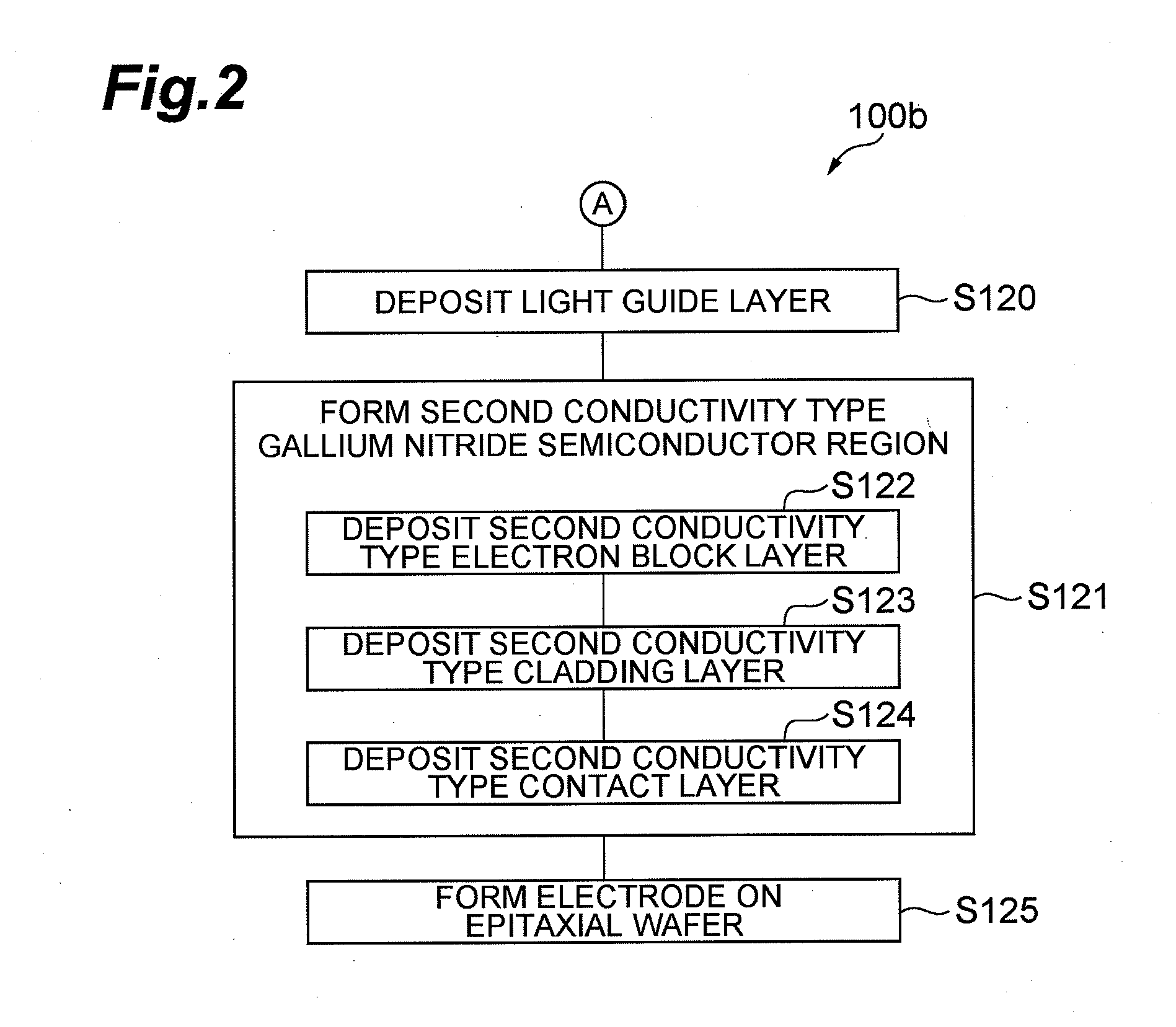
A method of making a nitride semiconductor laser comprises forming a first InGaN film for an active layer on a gallium nitride based semiconductor region, and the first InGaN film has a first thickness. In the formation of the first InGaN film, a first gallium raw material, a first indium raw material, and a first nitrogen raw material are supplied to a reactor to deposit a first InGaN for forming the first InGaN film at a first temperature, and the first InGaN has a thickness thinner than the first thickness. Next, the first InGaN is heat-treated at a second temperature lower than the first temperature in the reactor, while supplying a second indium raw material and a second nitrogen raw material to the reactor. Then, after the heat treatment, a second InGaN is deposited at least once to form the first InGaN film.

Description

BACKGROUND OF THE INVENTION[0001]1. Field of the Invention[0002]The present invention relates to a method of making a nitride semiconductor laser, a method of making an epitaxial wafer, and a nitride semiconductor laser.[0003]2. Related Background Art[0004]Patent document 1 (Japanese Patent Application No. 9-144291) discloses a method of forming a flat continuous GaN film. In the initial stage of deposition of the GaN film, the deposition for the GaN film is carried out under a film formation condition in the presence of a stoichiometrical excess amount of gallium (Ga). In the subsequent stage, the film is deposited under a film formation condition in the presence of a stoichiometrical excess amount of nitrogen (N). Over these stages, Ga and N are supplied onto a substrate in parallel.[0005]Patent document 2 (Japanese Unexamined Patent Application Publication No. 2000-49104) discloses a method of forming a satisfactory monocrystalline GaAsN. In this deposition process of a GaAsN mix...

Claims


Application Information

Patent Timeline
Patent Type & Authority Applications(United States)
IPC IPC(8): H01S5/323H01L21/20H01S5/343
CPCB82Y20/00H01L21/02389H01L21/02458H01S2304/04H01L21/0262H01S5/34333H01S2302/00H01L21/0254
Inventor UENO, MASAKIKYONO, TAKASHI
Owner SUMITOMO ELECTRIC IND LTD
Learn More