
Circuitized substrate with P-aramid dielectric layers and method of making same

a technology of p-aramid dielectric layer and circuitized substrate, which is applied in the direction of resistive material coating, nuclear engineering, railway components, etc., can solve the problems of increasing the relative complexity of various product designs, requiring more conductive layers and complex circuit designs, and fibrous materials occupying a relatively significant portion of the total volume of the substrate, so as to enhance the art of circuitized substrates

Inactive Publication Date: 2009-10-15
I3 ELECTRONICS
View PDF31 Cites 12 Cited by
  • Summary
  • Abstract
  • Description
  • Claims
  • Application Information

AI Technical Summary

Benefits of technology

The invention is about improving circuitized substrates by using a new dielectric material that has flame resistance, low moisture absorption, and no halogens. The method involves using p-aramid paper that is impregnated with a resin to form a layer that does not contain fiberglass fibers. The resulting circuitized substrate has improved performance and reliability.

Problems solved by technology

As is known in the industry, the relative complexity of various product designs has increased significantly in recent years.
Chip carriers, designed to carry one or more semiconductor chips thereon, also require more conductive layers and more complex circuit designs.
Such fibrous materials occupy a relatively significant portion of the substrate's total volume, a disadvantage especially when attempting to produce highly dense numbers of thru-holes and very fine line circuitry to meet new, more stringent design requirements.
If the glass is not removed, a loss of continuity might occur in the thru hole internal wall metal deposit.
In addition, both continuous and semi-continuous glass fibers add weight and thickness to the overall final structure, yet another disadvantage associated with such fibers.
Additionally, since lamination is typically at a temperature above 150° C., the resinous portion of the laminate usually shrinks during cooling to the extent permitted by the rigid copper cladding, which is not the case for the continuous strands of fiberglass or other continuous reinforcing material used.
The strands thus take on a larger portion of the substrate's volume following such shrinkage and add further to complexity of manufacture in a high density product.
Obviously, this problem is exacerbated as feature sizes (line widths and thicknesses, and thru-hole diameters) decrease.
Consequently, even further shrinkage may occur.
The shrinkage, possibly in part due to the presence of the relatively large volume percentage of continuous or semi-continuous fiberglass strands in the individual layers used to form a final product possessing many such layers, may have an adverse affect on dimensional stability and registration between said layers, adding even more problems for the PCB manufacturer.
Glass fiber presence, especially those of the woven type, also substantially impairs the ability to form high quality, very small thru-holes using a laser, one of the most preferred means to form such thru-holes.
This wide variation in encountered glass density leads to problems obtaining the proper laser power for each thru-hole and may result in wide variations in thru-hole quality, obviously unacceptable by today's very demanding manufacturing standards.
Glass fiber presence also often contributes to an electrical failure mode known as CAF growth.
CAF (cathodic / anodic filament) growth often results in time dependent electrical shorting failure which occurs when dendritic metal filaments grow along an interface (typically a glass fiber / epoxy resin interface), creating an electrical path between two features which should remain electrically isolated.
While the use of glass mattes composed of random discontinuous chopped fibers (in comparison to the longer fibers found in continuous structures) can largely abate the problem of inadequate laser drilled thru-hole quality, such mattes still contain fibers with substantial length compared to internal board feature spacing and, in some cases, offer virtually no relief from the problem of this highly undesirable type of growth.
With particular respect to many conventional chip carriers, which mount directly onto PCBs, if the coefficient of thermal expansion (CTE) of the semiconductor chip, the organic chip carrier, and the printed circuit board are substantially different from one another, industry standard semiconductor chip array interconnections to the organic chip carrier may be subject to high stress during thermal cycling operation, thus presenting another possible problem to the manufacturer of such substrates.
If solder ball connections (e.g., a ball grid array (BGA)) are used, as is well known, the formed solder interconnections between the organic chip carrier and printed circuit board may also be subject to high stress during operation.
Significant reliability concerns may then become manifest by failure of the connections or even failure of the integrity of the semiconductor chip (also known as chip “cracking”).
These reliability concerns significantly inhibit design flexibility.
For example, semiconductor chip sizes may be limited, or interconnect sizes, shapes and spacing may have to be customized beyond industry standards to reduce these stresses.
These limitations may limit the electrical performance advantages of the organic electronic package or add significant cost to the carrier-chip(s) electronic package.
This layer may be susceptible to stresses resulting from thermal cycling of the organic substrate together with a chip which is also solder coupled with the organic substrate.
If the redistribution layer cannot accommodate the thermal stresses, then the surface redistribution layer is also susceptible to deterioration, such as cracking, which can cause failure of interconnections between the carrier and chip, as well as between the carrier and PCB.
Safety concerns include the flammability of substitute products, meaning the ability of the final product to become inflamed or burn, e.g., due to the presence of excessive heat and / or when operating under extremely high electrical loads.
High shear forces exerted on the fibers during processing, e.g., refining, may cause damage to the fibers and adversely affect the CTE of the reinforcement.

Method used


Image

  • Circuitized substrate with P-aramid dielectric layers and method of making same
  • Circuitized substrate with P-aramid dielectric layers and method of making same
  • Circuitized substrate with P-aramid dielectric layers and method of making same

Examples


Embodiment Construction

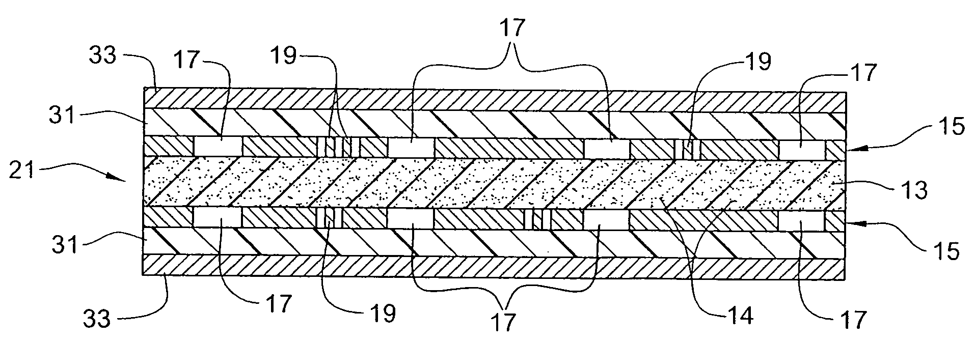
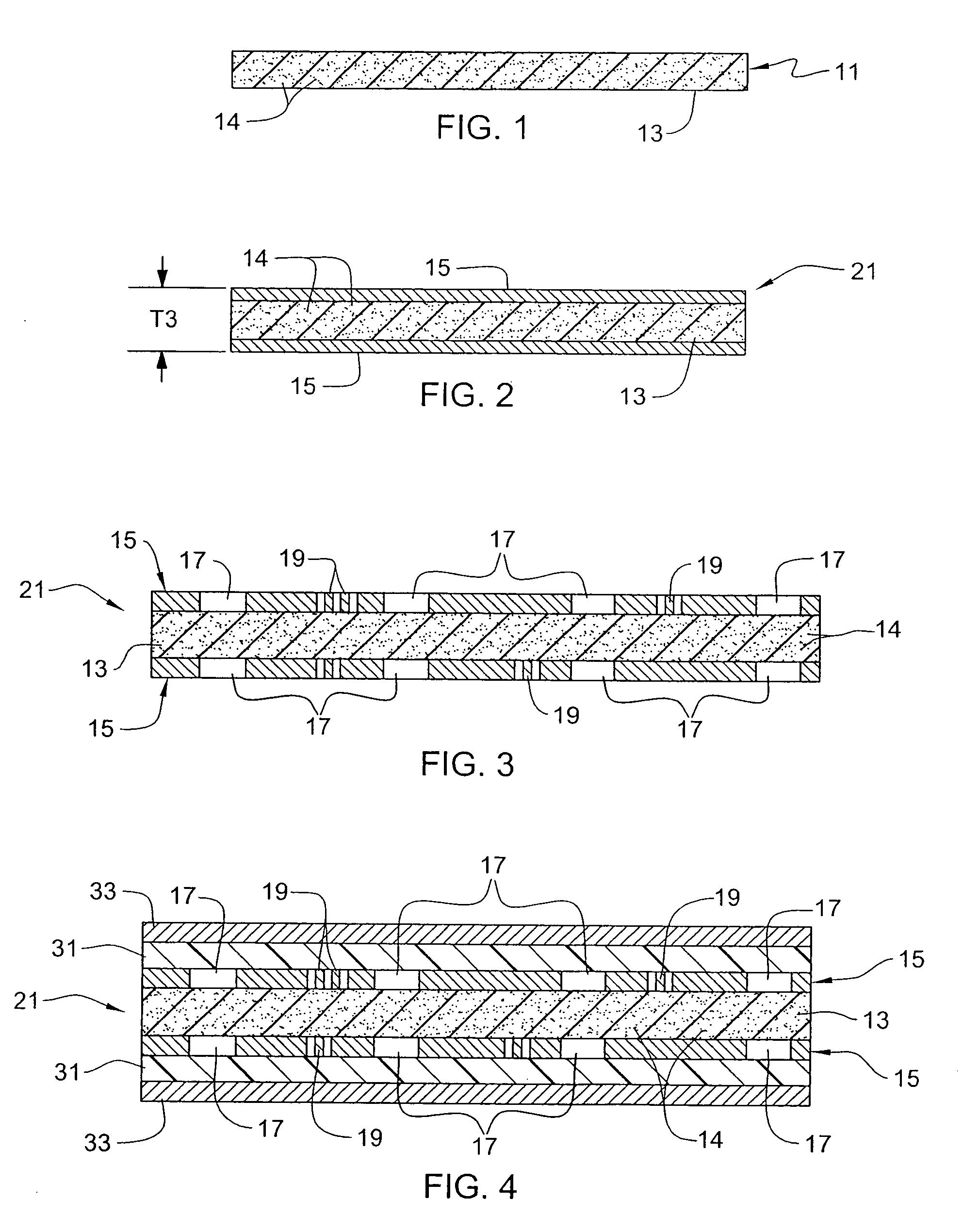
[0039]For a better understanding of the present invention, together with other and further objects, advantages and capabilities thereof, reference is made to the following disclosure and appended claims in connection with the above-described drawings. Like figure numbers will be used from figure to figure to identify like elements in these drawings.

[0040]By the term “circuitized substrate” as used herein is meant to include substrates having at least one (and preferably more) dielectric layer(s) of the new material defined herein and at least one (and preferably more) metal electrically conductive layer(s). It is believed that the teachings of the instant invention are also applicable to what are known as “flex” circuits.

[0041]By the term “electrical assembly” is meant at least one circuitized substrate as defined herein in combination with at least one electrical component electrically coupled thereto and forming part of the assembly. Examples of known such assemblies include chip ...


PUM

PropertyMeasurementUnit
thicknessaaaaaaaaaa
diameteraaaaaaaaaa
diameteraaaaaaaaaa

Abstract

A circuitized substrate including a dielectric layer having a p-aramid paper impregnated with a halogen-free, low moisture absorptivity resin and not including continuous or semi-continuous fiberglass fibers as part thereof, and a first circuitized layer positioned on the dielectric layer. A method of making this substrate is also provided.

Description

TECHNICAL FIELD[0001]This invention relates to circuitized substrates such as printed circuit boards (hereinafter also referred to simply as PCBs) and chip carriers and to processes for manufacturing same.CROSS REFERENCE TO CO-PENDING APPLICATIONS[0002]In Ser. No. 11 / 896,786, filed Sep. 6, 2007, there is defined a circuitized substrate which includes at least one circuit layer and at least one substantially solid dielectric layer comprised of a dielectric composition which includes a cured resin material and a predetermined percentage by weight of particulate fillers, but not including continuous or semi-continuous fibers as part thereof. Ser. No. 11 / 896,786 is a divisional application of Ser. No. 10 / 812,889, which is now U.S. Pat. No. 7,078,816 (see below).[0003]In Ser. No. 11 / 086,323, filed Mar. 23, 2005, there is defined a circuitized substrate including a composite layer having a first dielectric sub-layer including a plurality of fibers having a low coefficient of thermal expan...

Claims


Application Information

Patent Timeline
Patent Type & Authority Applications(United States)
IPC IPC(8): B05D5/12B05D3/06
CPCH01L23/145H01L23/4922H01L23/49822H01L23/49827H01L2924/12044H05K1/0366H01L2924/15311H05K3/4602H05K3/4652H05K2201/0209H05K2201/0278H01L2224/16225H05K1/0373
Inventor JAPP, ROBERT M.MARKOVICH, VOYA R.PAPATHOMAS, KOSTAS I.POLIKS, MARK D.
Owner I3 ELECTRONICS
Learn More