
Coating-type underlayer coating forming composition for lithography containing vinylnaphthalene resin derivative

a technology of vinylnaphthalene resin and coating type, applied in the direction of photosensitive materials, instruments, photomechanical equipment, etc., can solve the problems of affecting the effect of random reflection and standing wave of actinic rays on the substrate, and it is difficult to obtain a film thickness of resist pattern sufficient for substrate processing, so as to reduce the selection ratio and reduce the selection ratio of dry etching rate , the effect of preventing the collapse of resist pattern

Active Publication Date: 2009-10-08
NISSAN CHEM IND LTD
View PDF5 Cites 16 Cited by
  • Summary
  • Abstract
  • Description
  • Claims
  • Application Information

AI Technical Summary

Benefits of technology

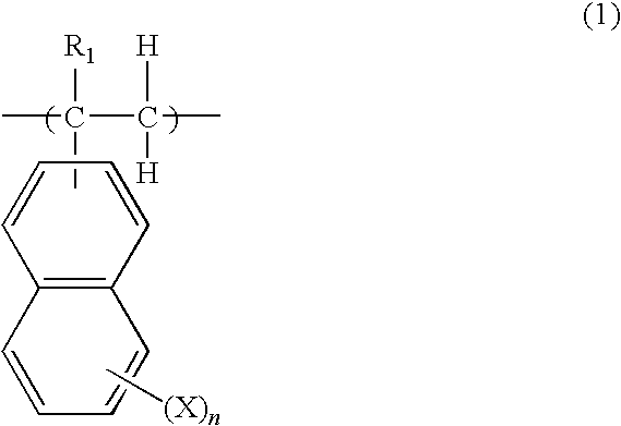
[0029]The present invention relates to a coating-type underlayer coating formed by use of a resin having a polymer of a vinylnaphthalene derivative in the main chain, and a coating-type underlayer coating forming composition for forming the coating-type underlayer coating.
[0030]The coating-type underlayer coating forming composition of the present invention can form a good pattern shape of photoresists without intermixing of the coating-type underlayer coating with the part applied thereon.
[0031]It is possible to confer a property for inhibiting effectively reflection from substrates on the coating-type underlayer coating forming composition of the present invention, and thus the coating-type underlayer coating can combine an effect as anti-reflective coating.
[0032]The coating-type underlayer coating forming composition of the present invention can provide excellent coating-type underlayer coatings that have a selection ratio of dry etching rate close to that of photoresists, a lower selection ratio of dry etching rate than that of photoresists, or a lower selection ratio of dry etching rate than that of semiconductor substrates.
[0033]In order to prevent collapse of resist pattern after development with miniaturization of resist pattern, it is performed to make photoresists thinner. The thin resists are required to be subjected to a process in which the resist pattern is transferred to the sublayer by etching process, and the substrate processing is performed by use of the sublayer as a mask, and a process in which the step comprising transferring the resist pattern to the sublayer by etching process, and transferring the pattern transferred to the sublayer to the layer applied below the sublayer with a different gas composition is repeated, and finally the substrate processing is performed. The coating-type underlayer coating and the composition for forming the same according to the present invention are effective for these processes. When the substrate processing is performed by use of the coating-type underlayer coating of the present invention, the coating-type underlayer coating has an etching resistance sufficiently against substrates to be processed (for example thermal silicon oxide coating, silicon nitride coating, polysilicon coating or the like on a substrate).
[0034]On the other hand, for obtaining fine resist pattern, it begins to be also used a process in which the resist pattern and the coating-type underlayer coating are made thinner on dry etching of coating-type underlayer coating than the width of pattern on the development of photoresists. The coating-type underlayer coating and the composition for forming the same according to the present invention are effective for this process, and has a selection property of dry etching rate close to that of photoresists.

Problems solved by technology

Along with this change, influences of random reflection and standing wave of actinic rays from a substrate have become serious problems.
When miniaturization of resist pattern progresses in future, problems such as a low resolution and collapse of resist pattern after development occur, and thus it is desired to make photoresists thinner.
Therefore, it is difficult to obtain a film thickness of resist pattern sufficient for the processing of substrates, and processes for providing a function as a mask in the substrate processing not only for resist pattern but also for coating-type underlayer coating formed between a resist and a semiconductor substrate to be processed become required.

Method used


Image

  • Coating-type underlayer coating forming composition for lithography containing vinylnaphthalene resin derivative
  • Coating-type underlayer coating forming composition for lithography containing vinylnaphthalene resin derivative
  • Coating-type underlayer coating forming composition for lithography containing vinylnaphthalene resin derivative

Examples


synthetic example 1

[0089]After 35 g (0.227 mol) of 2-vinylnaphthalene and 2.9 g (0.025 mol) of 2-hydroxyethyl acrylate were dissolved in 112 g of cyclohexanone in a flask, the atmosphere in the flask was substituted with nitrogen, and the temperature was raised to 60° C. After the completion of rise in temperature, 1.9 g of azobisisobutyronitrile dissolved in 47 g of cyclohexanone was added under pressure with nitrogen, and reacted with at 60° C. for 24 hours. The reacted solution was cooled and then added into methanol. Thereby a polymer was re-precipitated, and dried with heating to obtain the polymer of formula [5-1]. The resulting polymer had a weight average molecular weight Mw of 12000 (in terms of standard polystyrene).

synthetic example 2

[0090]After 10 g (0.065 mol) of 2-vinylnaphthalene and 23.0 g (0.097 mol) of 3-hydroxy-2-adamatyl methacrylate (manufactured by Maruzen Petrochemical, trade name: HAMA) were dissolved in 97 g of cyclohexanone in a flask, the atmosphere in the flask was substituted with nitrogen, and the temperature was raised to 60° C. After the completion of rise in temperature, 1.6 g of azobisisobutyronitrile dissolved in 41 g of cyclohexanone was added under pressure with nitrogen, and reacted with at 60° C. for 24 hours. The reacted solution was cooled and then added into methanol. Thereby a polymer was re-precipitated, and dried with heating to obtain the polymer of formula [5-2]. The resulting polymer had a weight average molecular weight Mw of 16000 (in terms of standard polystyrene).

synthetic example 3

[0091]After 30 g (0.195 mol) of 2-vinylnaphthalene and 3.1 g (0.022 mol) of glycidyl methacrylate were dissolved in 98 g of cyclohexanone in a flask, the atmosphere in the flask was substituted with nitrogen, and the temperature was raised to 60° C. After the completion of rise in temperature, 1.7 g of azobisisobutyronitrile dissolved in 41 g of cyclohexanone was added under pressure with nitrogen, and reacted with at 60° C. for 24 hours. The reacted solution was cooled and then added into methanol. Thereby a polymer was re-precipitated, and dried with heating to obtain the polymer of formula [5-3]. The resulting polymer had a weight average molecular weight Mw of 10000 (in terms of standard polystyrene).

[0092]After 15 g of the polymer of formula [5-3] and 2.0 g (0.009 mol) of 9-anthracene carboxylic acid were dissolved in 68 g of cyclohexanone, 0.05 g of benzyltriethyl ammonium chloride was added, and reacted with at 130° C. for 24 hours to obtain a solution containing the polymer ...


PUM

PropertyMeasurementUnit
molar ratioaaaaaaaaaa

Abstract

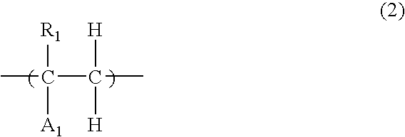
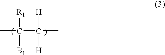
[Object] To provide a coating-type underlayer coating forming composition that is applied for multi-ply coating process by thin film resist in order to prevent collapse of resist pattern after development with miniaturization of resist pattern, and that shows a sufficient etching resistance against a semiconductor substrate to be processed on processing of the substrate by having a low dry etching rate compared with the photoresist and substrate.[Means for solving problems] A coating-type underlayer coating forming composition that is used for lithography process by multiply coating, comprising a polymer containing a vinylnaphthalene based structural unit and an acrylic acid based structural unit containing an aromatic hydroxy group or a hydroxy-containing ester. A coating-type underlayer coating forming composition further comprising an acrylic acid based structural unit containing an aliphatic cyclic compound-containing ester or an aromatic compound-containing ester.

Description

TECHNICAL FIELD[0001]The present invention relates to a coating-type underlayer coating forming composition for lithography that is effective on processing of semiconductor substrates, and a method for forming photoresist pattern by use of the coating-type underlayer coating forming composition.BACKGROUND ART[0002]Conventionally, in the manufacture of semiconductor devices, micro-processing by lithography using a photoresist composition has been carried out. The micro-processing is a processing method comprising forming a thin film of a photoresist composition on a substrate to be processed, such as a silicon wafer or the like, irradiating actinic rays such as ultraviolet rays through a mask pattern on which a pattern for a semiconductor device is depicted, developing it to obtain a photoresist pattern, and etching the substrate to be processed, such as a silicon wafer or the like by use of the photoresist pattern as a protective film. However, in recent progress in high integration...

Claims


Application Information

Patent Timeline
Patent Type & Authority Applications(United States)
IPC IPC(8): G03F7/004C08F220/26C08F224/00C08F8/00C08L37/00C08L33/08G03F7/20H01L21/31
CPCG03F7/11G03F7/091
Inventor SAKAGUCHI, TAKAHIROENOMOTO, TOMOYUKI
Owner NISSAN CHEM IND LTD
Learn More