Silicon substrate and manufacturing method thereof

a technology of silicon substrate and manufacturing method, which is applied in the direction of crystal growth process, crystal growth process, polycrystalline material growth, etc., can solve the problems of significant deterioration of the electric characteristics of the solid-state imaging device, deterioration of the device characteristics, so as to prevent the reduction of the concentration of carbon, prevent the occurrence of a reduction in the gettering capability, and prevent the effect of carbon concentration

Active Publication Date: 2009-09-10
SUMCO CORP
View PDF14 Cites 10 Cited by
  • Summary
  • Abstract
  • Description
  • Claims
  • Application Information

AI Technical Summary

Benefits of technology

[0041]When the second silicon substrate is used to manufacture a solid-state imaging device, it is possible to getter heavy metal in a portion of the substrate doped with carbon and prevent contaminated heavy metal from being segregated on the n+ implantation layer, serving as a phosphorus getter. In addition, a gettering portion is not formed by ion implantation, but is formed over the entire thickness of the substrate before an epitaxial layer is formed. Therefore, in the second silicon substrate, it is possible to prevent carbon from being diffused by a heat treatment of the subsequent process and prevent the concentration of carbon from being lowered. As a result, it is possible to prevent a reduction in gettering capability. In this way, it is possible to prevent the

Problems solved by technology

When impurities, such as heavy metal, are mixed with the silicon substrate, electrical characteristics of the solid-state imaging device significantly deteriorate due to, for example, the generation of white spots.
However, when an n/n+/n substrate used for a device that is operated at high speed, such as a CCD (charge coupled device) or a CIS (CMOS image sensor) is manufactured, there is a problem in that device characteristics deteriorate.
As a result, device characteristics deteriorate.
Therefore, the intrinsic gettering method requires multi-stage heat treatment processes, which result in an increase in manufacturing costs.
In addition, in the intrinsic gettering method, a heat treatment needs to be performed at a high temperature for a long time.
Therefore, there is a concern that the metal contamination of a silicon substrate will increase during a heat treatment process or between the heat treatment processes.
On the oth

Method used


Image

  • Silicon substrate and manufacturing method thereof
  • Silicon substrate and manufacturing method thereof
  • Silicon substrate and manufacturing method thereof

Examples


first embodiment

[0056]Hereinafter, a silicon substrate according to a first embodiment of the present invention will be described with reference to the accompanying drawings.

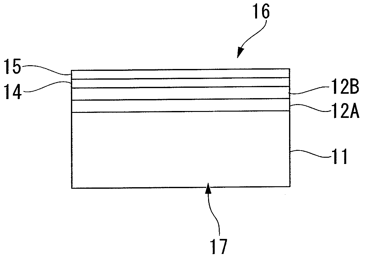
[0057]FIGS. 1A to 1D are front cross-sectional views illustrating a silicon substrate in each step of a method of manufacturing a first silicon substrate according to the first embodiment. In FIGS. 1A to 1D, reference numeral 11 denotes a silicon substrate.

[0058]In order to obtain the silicon substrate 11 shown in FIGS. 1A to 1D, first, polysilicon, which is a raw material of a single crystal silicon, is placed in a vitreous silica crucible, and a predetermined amount of graphite powder is applied on the surface of the polysilicon. At the same time, boron (B) is injected as a dopant, and a CZ crystal having carbon added thereto is pulled up in a hydrogen atmosphere by the Czochralski method (CZ method), which will be described below.

[0059]The CZ crystal is a single crystal silicon that is manufactured by the Czochralski method ...

second embodiment

[0139]Hereinafter, a silicon substrate according to a second embodiment of the present invention will be described with reference to the accompanying drawings.

[0140]The second embodiment of the present invention relates to a second silicon substrate and a method of manufacturing the same, and more particularly, to a technique applicable for a silicon substrate for a solid-state imaging device that can improve gettering capability regardless of a heat treatment of a device step and is used to manufacture a solid-state imaging device.

[0141]FIGS. 7A to 7D are front cross-sectional views illustrating a silicon substrate in each step of a method of manufacturing a silicon substrate according to this embodiment, and FIG. 13 is a flowchart illustrating the method of manufacturing a silicon substrate according to this embodiment. In the drawings, reference numeral 21 denotes a silicon substrate.

[0142]As shown in FIG. 13, the method of manufacturing a silicon substrate according to this embo...


PUM


Abstract

A silicon substrate is manufactured from a single crystal silicon that is doped with phosphorus (P) and is grown by a CZ method to have a predetermined carbon concentration and a predetermined initial oxygen concentration. An n+ epitaxial layer or an n+ implantation layer that is doped with phosphorus (P) at a predetermined concentration or more is formed on the silicon substrate. An n epitaxial layer that is doped with phosphorus (P) at a predetermined concentration is formed on the n+ layer.

Description

BACKGROUND OF THE INVENTION[0001]1. Field of the Invention[0002]The present invention relates to a silicon substrate and a method of manufacturing the same, and more particularly, to a technique applicable for a silicon substrate for a solid-state imaging device that has high gettering capability and is used to manufacture a solid-state imaging device.[0003]Priority is claimed on Japanese Patent Application No. 2008-054840, filed Mar. 5, 2008, and Japanese Patent Application No. 2008-054841, filed Mar. 5, 2008, the content of which is incorporated herein by reference.[0004]2. Description of Related Art[0005]A solid-state imaging device is manufactured by slicing a single crystal silicon pulled by, for example, a CZ (Czochralski) method into a silicon substrate and forming a circuit on the silicon substrate. When impurities, such as heavy metal, are mixed with the silicon substrate, electrical characteristics of the solid-state imaging device significantly deteriorate due to, for exa...

Claims


Application Information

Patent Timeline
IPC IPC(8): H01L29/167H01L21/203
CPCC30B15/00H01L27/146H01L21/3221C30B29/06H01L21/20C30B15/04
Inventor KURITA, KAZUNARIOMOTE, SHUICHI
Owner SUMCO CORP
Why Eureka
Try Eureka