
Methods of Treating a Surface to Promote Binding of Molecule(s) of Interest, Coatings and Devices Formed Therefrom

Inactive Publication Date: 2009-03-05
ATOTECH DEUT GMBH
View PDF99 Cites 14 Cited by
  • Summary
  • Abstract
  • Description
  • Claims
  • Application Information

AI Technical Summary

Benefits of technology

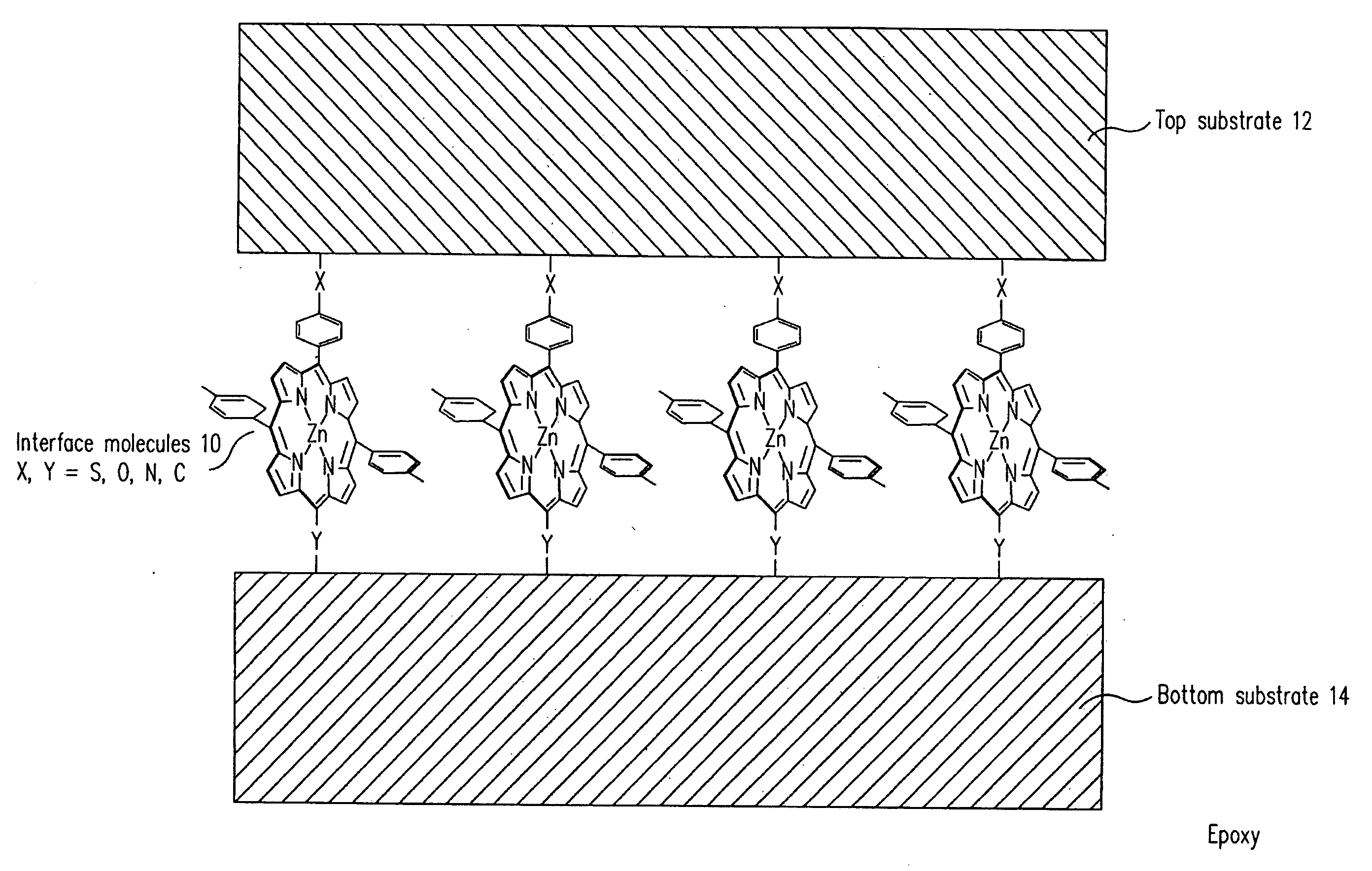
[0024]In some aspects, the present invention provides a method of treating a surface to promote binding of one or more molecules of interest to the surface, comprising the steps of: contacting the surface with an organic molecule comprising a thermally stable base bearing one or more attachment groups configured to attach the organic molecule to the surface and one or more binding groups configured to bind the organic molecule to a subsequent material of interest and; and heating the organic molecule and surface to a temperature of at least 25° C. wherein the organic molecules attach to the surface, and exhibit enhanced affinity for binding the subsequent material of interest.
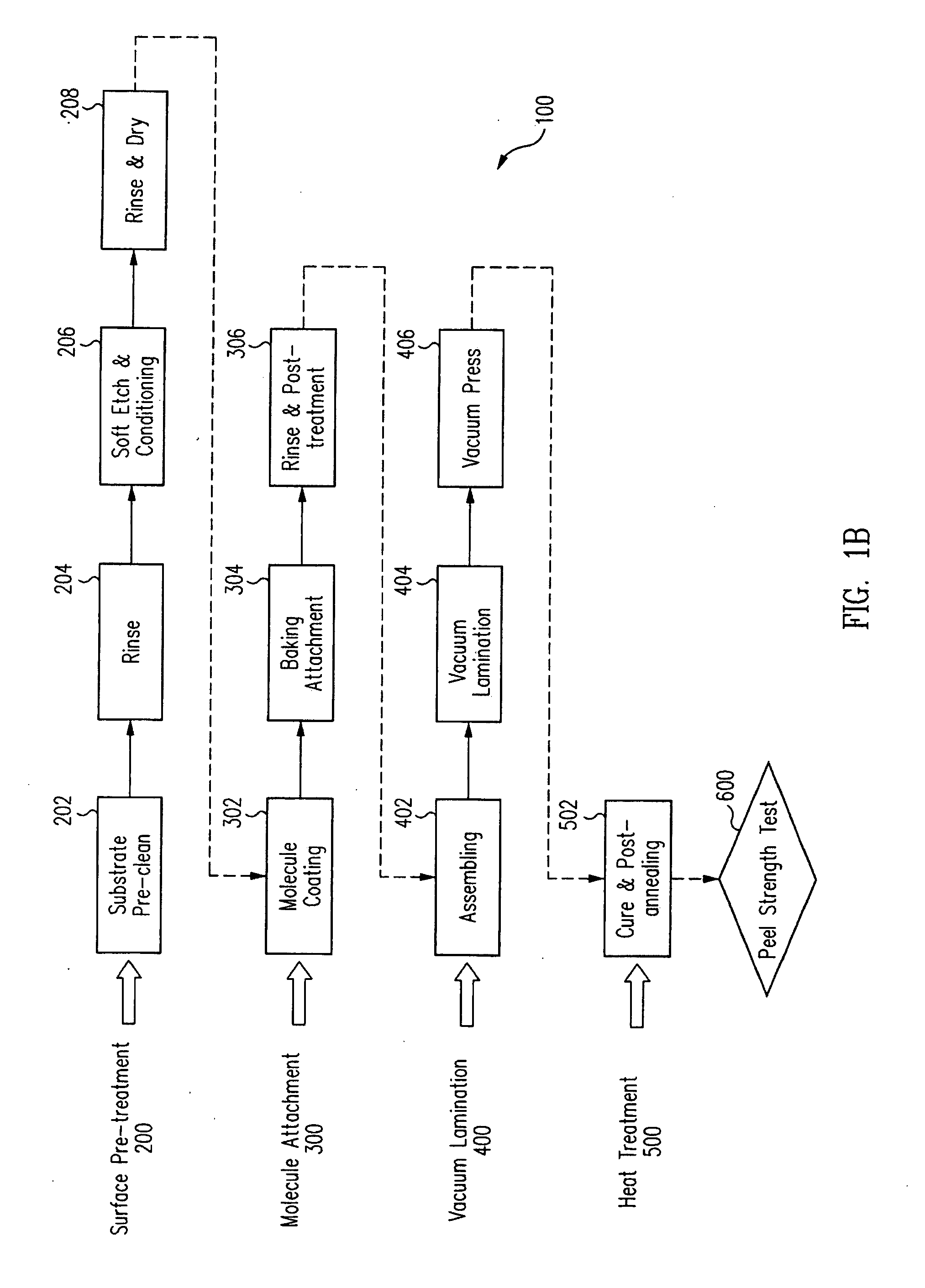
[0026]In another aspect, embodiments of the present invention provide for additional cleaning, baking, etching, chemical oxidation or other pre-treatment of the surface prior to the deposition or attachment of the molecule to enhance the deposition of the molecule, the reaction of the molecule to the surface, or the ability of the surface to bond with the molecules as deposited.
[0027]In other aspects, embodiments of the present invention provide structures or films of organic molecular layers that promote favorable deposition or attachment of metal elements or molecules on surfaces which may be advantageously employed in many processes.

Problems solved by technology

These may especially be unstable functional groups, formed transiently, for instance radicals formed by vigorous oxidation of the surface, either chemically or via irradiation.
Additionally, in many cases, such as where the surface or the molecule of interest must be modified in order to be feasible, such modification methods require relatively complex and expensive pretreatments, such as the use of vacuum installations for the plasma methods such as chemical vapor deposition (CVD), the technique of plasma assisted chemical vapor deposition (PACVD), irradiation, etc., which, moreover, do not necessarily preserve the chemical, integrity of the precursors.
Therefore, it is much more difficult to use the same organic chemistry reactions to attach an organic molecule of interest onto a metallic surface.
However, these reactions cannot be exploited in all situations.
As device densities increase, high density package designs such as multi-layer structures are becoming increasingly important, which present additional design challenges.
Fabrication steps of PCB and semiconductor devices are costly and complicated and improvements are highly sought.
The patterning of very fine metal lines is a particular challenge.
Many conventional deposition processes do not consistently fill semiconductor structures in which the aspect ratios exceed 6:1, and particularly when the aspect ratios exceed 10:1.
As such, there is a great amount of ongoing effort being directed to the formation of void-free, nanometer-sized structures having aspect ratios of 6:1 or higher.
However, as the feature sizes become smaller, if becomes difficult to have adequate seed step coverage with PVD techniques, as discontinuous islands of copper agglomerates are often obtained in the feature side walls close to the feature bottom.
When the deposition thickness on the field is reduced to prevent throat closure, ALD and CVD techniques are also prone to generate discontinuities in the seed layer.
These discontinuities in the seed layer have been shown to cause plating defects in the layers plated over the seed layer.
In addition, copper tends to oxidize readily in the atmosphere and copper oxide readily dissolves in the plating solution.
Another challenge with direct copper plating on a suitable barrier metal layer is that the resistance of the barrier metal layer is high (low conductivity) and is known to cause high edge-plating; i.e. thicker copper plating at the edge of the substrate and no copper plating in the middle of the substrate.
Also, copper tends to plate on local sites of nucleation, resulting in clusters of copper nuclei, copper clusters / crystal, so deposition is not uniform on the whole surface of the substrate.
Many of these connections suffer from failures due to poor adhesion between top metal layers and underling metal or insulator layers.
Additionally, adhesion of PCB substrates (such as epoxy PCB substrates) onto metal layers in PCB manufacturing continues to present significant challenges to the industry.
Similar issues are found in a wide variety of electronic materials, including flexible substrates, liquid crystal display (LCD) and plasma displays, solar panels, and the like.

Method used


Image

  • Methods of Treating a Surface to Promote Binding of Molecule(s) of Interest, Coatings and Devices Formed Therefrom
  • Methods of Treating a Surface to Promote Binding of Molecule(s) of Interest, Coatings and Devices Formed Therefrom
  • Methods of Treating a Surface to Promote Binding of Molecule(s) of Interest, Coatings and Devices Formed Therefrom

Examples


example 1

Molecule Attachment on a Metal Substrate

[0163]This example illustrates one exemplary approach to form a layer of organic molecules on a metal substrate. In this instance, a thiol-linker molecule 16 shown in FIG. 3, is attached to copper surface via the formation of C—S—Cu bond, as illustrated in FIGS. 1A and 2. A commercial copper wafer substrate was first cleaned by sonication for 5 minutes in acetone, water and then isopropyl alcohol. The substrate was coated with a solution containing 1 mM of the porphyrin molecule in ethanol by spin-coating. The sample was then baked at 150° C. for 5 minutes and followed by solvent rinse to remove the residual unreacted molecules. The amount of molecule attached can be adjusted by varying the concentration of the molecule, the attachment temperature, and duration, and quantified by Cyclic Voltammetry (CV) shown in FIG. 4, which is based on the redox property of porphyrin molecule as described in (Roth, K. M., Gryko, D. T. Clausen, C. Li, J., Lin...

example 2

Molecule Attachment on Semiconductor Substrates

[0164]This example illustrates another exemplary approach to form a layer of organic molecules on semiconductor substrates (SS): (a) Si, (b) TiN, (c) TiW, and (d) WN. In this instance; a hydroxy-linker molecule 1006 is attached to semiconductor surface via the formation of C—O—SS bond. Commercial semiconductor wafer substrates were first cleaned by sonication for 5 minutes in acetone, water, and then isopropyl alcohol. The substrates were coated with a solution containing 1 mM of the porphyrin molecule in benzonitrile by spin-coating. The sample was then baked at 350° C. for 5 minutes and followed by solvent rinse to remove the residual unreacted molecules. As illustrated in FIG. 5, the attachment of a molecular layer on each substrate is demonstrated again by the porphyrin CV signature peaks.

example 3

Molecule Attachment on Semiconductor Barrier Substrates

[0165]This example illustrates another exemplary approach to form a layer of organic molecules on semiconductor barrier substrates (BS) Ta and TaN. In this instance, a hydroxy-linker molecule 258 is attached to semiconductor surface via the formation of C—O—BM bond. Commercial barrier wafer substrates were first cleaned by sonication for 5 minutes in acetone, water, and then isopropyl alcohol. The substrates were coated with a solution, containing 1 mM of the porphyrin molecule in benzonitrile by spin-coating. The sample was then baked at 350° C. for 5 minutes and followed by solvent rinse to remove the residual unreacted molecules. In this case, the molecular layer formed can not be characterized by CV since the barrier substrates are electrically poorly conductive. The molecular layer was characterized by Laser Desorption Time-of-Flight Mass Spectroscopy (LDTOF) instead. FIG. 6 shows; exemplary LDTOF spectra that match the sta...


PUM

PropertyMeasurementUnit
Temperatureaaaaaaaaaa

Abstract

The present invention generally relates to methods of treating a surface of a substrate, and to the use of the method and resulting films, coatings and devices formed therefrom in various applications including but not limited to electronics manufacturing, printed circuit board manufacturing, metal electroplating, the protection of surfaces against chemical attack, the manufacture of localized conductive coatings, the manufacture of chemical sensors, for example in the fields of chemistry and molecular biology, the manufacture of biomedical equipment, and the like. In another aspect, the present invention provides a printed circuit board, a printed circuit board, comprising: at least one metal layer; a layer of organic molecules attached to the at least one metal layer; and an epoxy layer atop said layer of organic molecules.

Description

RELATED APPLICATIONS[0001]This patent application claims the benefit of, and priority to, U.S. Provisional Patent Application Ser. No. 60 / 969,468, filed on Aug. 31, 2007, titled “Methods of Treating a Surface to Promote Binding of Molecule(s) of Interest, Coatings and Devices Formed Therefrom,” the disclosure of which is hereby incorporated by reference in its entirety. This patent application is related to U.S. patent application Ser. No. 11 / 848,860, filed on Aug. 31, 2007, titled “Methods of Treating a Surface to Promote Metal Plating and Devices Formed,” the disclosure of which is hereby incorporated by reference in its entirety.TECHNICAL FIELD[0002]The present invention generally relates to methods of treating a surface of a substrate, and to the use of the method and resulting films, coatings, and devices formed therefrom in variousapplications including but not limited to electronics manufacturing, printed circuit board manufacturing, metal electroplating, the protection of su...

Claims


Application Information

Patent Timeline
IPC IPC(8): H05K1/03C25D5/02C23C16/513C23C14/00B32B37/00H05K1/00C08J7/043C08J7/044C08J7/056
CPCH05K2203/1105H05K2203/121C08J7/065C08J7/12C09J5/02C23C18/1653Y10T156/10C23C18/1893C23C18/2066H05K3/181H05K3/389H05K3/4611C23C18/1844Y02P20/582C08J7/043C08J7/044C08J7/056
Inventor KUHR, WERNER G.SHI, STEVEN Z.WEI, JEN-CHIEHLIU, ZHIMINGWEI, LINGYUN
Owner ATOTECH DEUT GMBH
Learn More