
Materials for photoresist, photoresist composition and method of forming resist pattern

a technology of resist pattern and composition, applied in the field of materials for photoresist, photoresist composition and method of forming resist pattern, can solve the problems of reducing throughput, difficulty in achieving required processing accuracy, and higher defect occurrence rate due to foreign material disadvantageous, etc., to achieve high sensitivity, low line edge roughness, and high resolution

Inactive Publication Date: 2008-04-03
TOKYO OHKA KOGYO CO LTD +1
View PDF3 Cites 6 Cited by
  • Summary
  • Abstract
  • Description
  • Claims
  • Application Information

AI Technical Summary

Benefits of technology

The present invention provides a material for photoresist that can solve the problems of LER (irregularities) and sensitivity in semiconductor fabrication. The material is a mixture of compounds with zero to six functional groups that are chemically converted due to an action of an acid with the reduced solubility in an alkaline developer. The material has a structure in which two or more triphenyl methane structures are bonded in the nonconjugated state to a section other than the functional groups, and each of the functional groups is bonded to a phenolic hydroxy group of a polynuclear phenol compound. The polynuclear phenol compound has high resistance against etching and can form an amorphous film. The material can be used in negative-tone photoresist compositions and has a low molecular weight, but the molecular weight should not be too small or too large.

Problems solved by technology

In recent years, in association with the necessity of fabrication at increasingly smaller dimensions, the LER becomes relatively more visible, and achievement of required processing accuracy has become more and more difficult.
Furthermore, in the photo lithography or in the electron beam lithography, when a numerical aperture in a drawn portion becomes higher, a defect occurrence rate due to a foreign material disadvantageously becomes higher, and also in the electron beam lithography, there occurs the problem of lower throughput, so that also a negative-tone resist is required.
In a case of the resist using chloromethylated calixarene, development is performed with an organic solvent, and therefore there are the problems of toxity and inflammability.
There is also the problem that the resist can hardly be applied to a mass production line of semiconductors, because development is generally performed with an alkaline aqueous solution.

Method used


Image

  • Materials for photoresist, photoresist composition and method of forming resist pattern
  • Materials for photoresist, photoresist composition and method of forming resist pattern
  • Materials for photoresist, photoresist composition and method of forming resist pattern

Examples


first embodiment

[0062]In a first embodiment, a method of obtaining materials for photoresist (A1, A2, and A3) by column chromatography according to the present invention is described.

[0063]In a first step (for an etherification), polynuclear phenolic compound 3M6C-MBSA (15 g) and potassium carbonate (7 g) were added to acetone (300 ml), and the mixture was sufficiently stirred. Then a solution prepared by adding a-bromo-γ-butylolactone (4.0 g) in acetone solution (50 ml) was added to the mixture at the room temperature, and the mixed solution was stirred for two hours at the temperature of 45 degrees C. After the reaction is completed, acetone was removed from the solution by evapolation under the reduced pressure, water (250 ml) and ethyl acetate (205 ml) were added to the solution, and the solution was sufficiently shaken in 1L separating funnel. An organic layer was recovered, washed with water (300 ml), concentrated, vacuum-dried, and polynuclear phenolic compound (17 g) was obtained. High-perf...

second embodiment

[0068]In this embodiment, a method for synthesizing a material for photoresist (A4) in which δ-hydroxycarboxylic acid is introduced into 3M6C-MBSA (X1).

[0069]In the first step (for etherification), polynuclear phenolic compound X1 (15 g) and potassium carbonate were added to acetone (300 ml), and stirred sufficiently. a-bromo-γ-valerolactone (4.0 g) in acetone (50 ml) was added at the room temperature, and the solution was stirred for two hours at the temperature of 45 degrees C. After the reaction was completed, acetone was removed by evapolation under the reduced pressure, water (250 ml) and ethyl acetate (250 ml) were added, and shaken sufficiently in a 1L separating funnel. The organic layer was recovered, washed with water (300 ml), concentrated, vacuum-dried, and an ether compound of the polynuclear phenolic compound X1 (17 g) was obtained. HPLC analysis was performed to find that etherification rate was 1.2 per 1 molecule on average, and specifically, a percentage of X1 havin...

third embodiment

[0072]In a third embodiment, a method for a pattern forming using the material for photoresist according to the present invention is described.

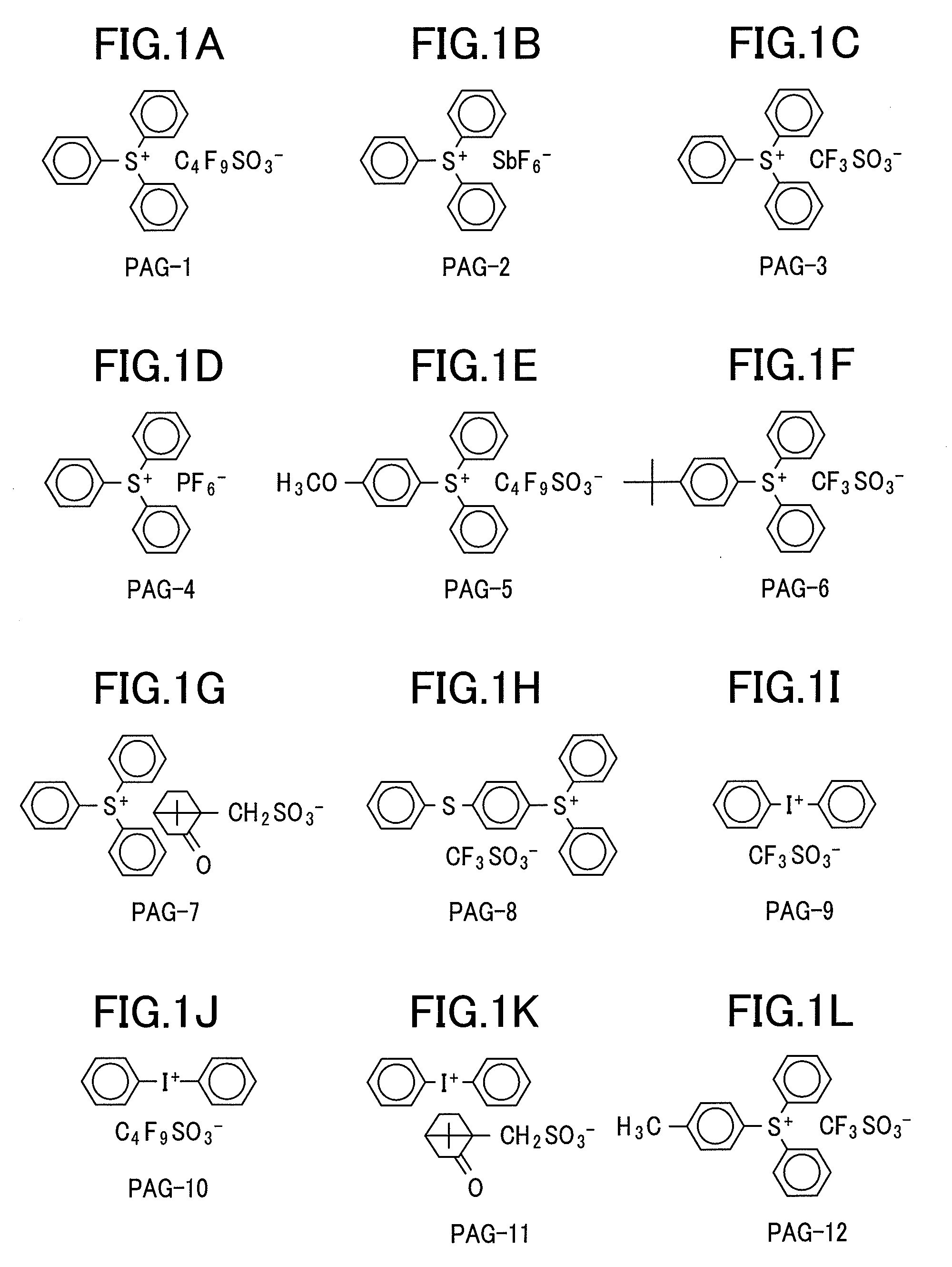
[0073]The material for photoresist A1, 100 weight portions, and 5 weight portions for triphenyl sulfonium triflate acid generator synthesized in the first embodiment were dissolved into weight 500 for propylene glycol monomethyl ether acetate (PGMEA), filtered by the filter having the diameter of 0.20 micrometers to obtain a solution of the photoresist compound.

[0074]The photoresist solution was spin-coated to a silicon substrate processed with hexamethyl disilazane, subjected for a thermal processing for two minutes at the temperature of 100° C., and a resist film having the thickness of 0.20 micrometers was formed. A line and space pattern is drawn on the resist film on the substrate with an electron beam lithography system with the acceleration voltage of 50 kV at an irradiation dose of 10 μC / cm2. Then the resist film was subjected to ther...


PUM

PropertyMeasurementUnit
weight ratioaaaaaaaaaa
sizeaaaaaaaaaa
wavelengthaaaaaaaaaa

Abstract

To overcome the problem that a device performance is degraded by the edge roughness of a photoresist pattern, a mixture of polynuclear phenol compounds having, in one molecule, 0 to 6 functional groups which are chemically converted due to actions of an acid with the solubility in an alkaline developer reduced is used as a material for photoresist. In the mixture, two or more triphenyl methane structures are bonded to portions other than the functional group in the nonconjugated state. Furthermore, the mixture comprises polynuclear compounds with the average number of functional groups of 2.5 or below and includes the polynuclear compounds not having any functional group per molecule by 15% or less in the term of weight ratio, and the polynuclear phenol compounds having 3 or more functional groups per molecule by 40% or less.

Description

CLAIM OF PRIORITY[0001]The present application claims priority from JP 2006-267830 filed on Sep. 29, 2006, the content of which is hereby incorporated by reference into this application.BACKGROUND OF THE INVENTION[0002]1. Field of the Invention[0003]The present invention relates to negative-tone photoresist compositions used in extremely fine processing of a semiconductor device using extreme ultraviolet light (EUV light), materials for forming patterns used in the negative-tone resist compositions, and a method of patterns on a semiconductor device fabricated by using the negative-tone photoresist compositions.[0004]2. Descriptions of the Related Arts[0005]Nanofabrication by lithography using a photoresist is performed in a semiconductor device manufacturing process. In association with the recent tendency for a higher degree of circuit integration, fine patterns with the size less than 100 nanometers are often formed. A wavelength of beams or rays used for exposure has been increa...

Claims


Application Information

Patent Timeline
Patent Type & Authority Applications(United States)
IPC IPC(8): G03C1/10C07C39/12G03F7/20C07C59/52
CPCC07C39/15G03F7/0382C07C39/17Y10S430/106
Inventor KOJIMA, KYOKOHADA, HIDEOSHIONO, DAIJU
Owner TOKYO OHKA KOGYO CO LTD
Learn More