
Method for manufacturing ferroelectric memory device and ferroelectric memory device

a technology of ferroelectric memory and memory device, which is applied in the direction of capacitors, semiconductor devices, electrical devices, etc., can solve the problems of ferroelectric capacitors deteriorating by hydrogen, ferroelectric film damage, and difficulty in forming contact holes securely in a manner to reach the upper electrode, so as to prevent the deterioration of the characteristics of ferroelectric capacitors

Inactive Publication Date: 2007-09-13
SEIKO EPSON CORP
View PDF21 Cites 2 Cited by
  • Summary
  • Abstract
  • Description
  • Claims
  • Application Information

AI Technical Summary

Benefits of technology

[0011]In accordance with an advantage of some aspects of the invention, it is possible to provide a ferroelectric memory device and a method for manufacturing a ferroelectric memory device, in which deterioration of characteristics of a ferroelectric capacitor due to generation of hillocks can be prevented, and formation of a contact hole to reach an upper electrode is facilitated, thereby further preventing degradation of the characteristics of the ferroelectric capacitor.

Problems solved by technology

For such ferroelectric memory devices, it has become an important issue to prevent deterioration of ferroelectric films in their manufacturing process.
When the ferroelectric capacitor is formed through etching, its ferroelectric film may be damaged.
When hillocks are formed on the upper electrode in this manner, when a hydrogen barrier film is formed to cover the ferroelectric capacitor, the hydrogen barrier film cannot be formed well on the upper electrode that has the hillocks formed thereon, and the upper electrode cannot be sufficiently covered by the hydrogen barrier film, such that the ferroelectric capacitor would eventually be deteriorated by hydrogen.
When forming the contact hole by etching to reach the upper electrode, it would be difficult to form the contact hole securely in a manner to reach the upper electrode if the hydrogen barrier film that covers the upper electrode is composed of a material that is difficult to be etched.
However, by so doing, the upper electrode may be largely cut in part, which leads to degradation of the characteristics of the ferroelectric capacitor.
For forming a contact hole that reaches the upper electrode, excessive over-etching may have been needed in the past, for example, when the upper electrode is covered by a hydrogen barrier film composed of a material that is difficult to be etched.
Because titanium oxide such as titania (TiO2) is difficult to be etched, and is therefore difficult to be patterned, it was thought that titanium oxide could not be used as a hard mask.

Method used


Image

  • Method for manufacturing ferroelectric memory device and ferroelectric memory device
  • Method for manufacturing ferroelectric memory device and ferroelectric memory device
  • Method for manufacturing ferroelectric memory device and ferroelectric memory device

Examples


Embodiment Construction

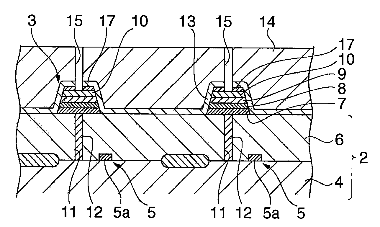
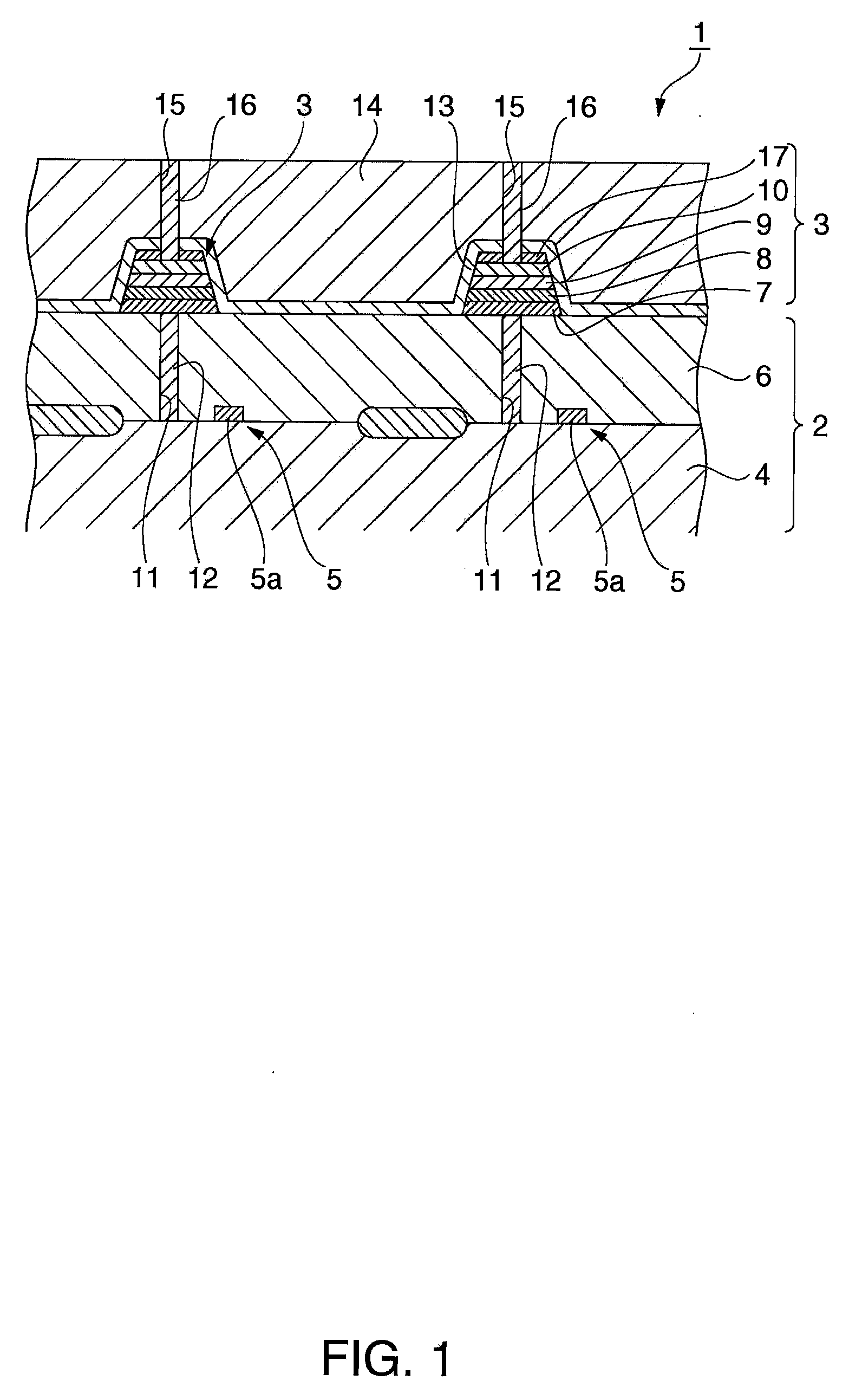
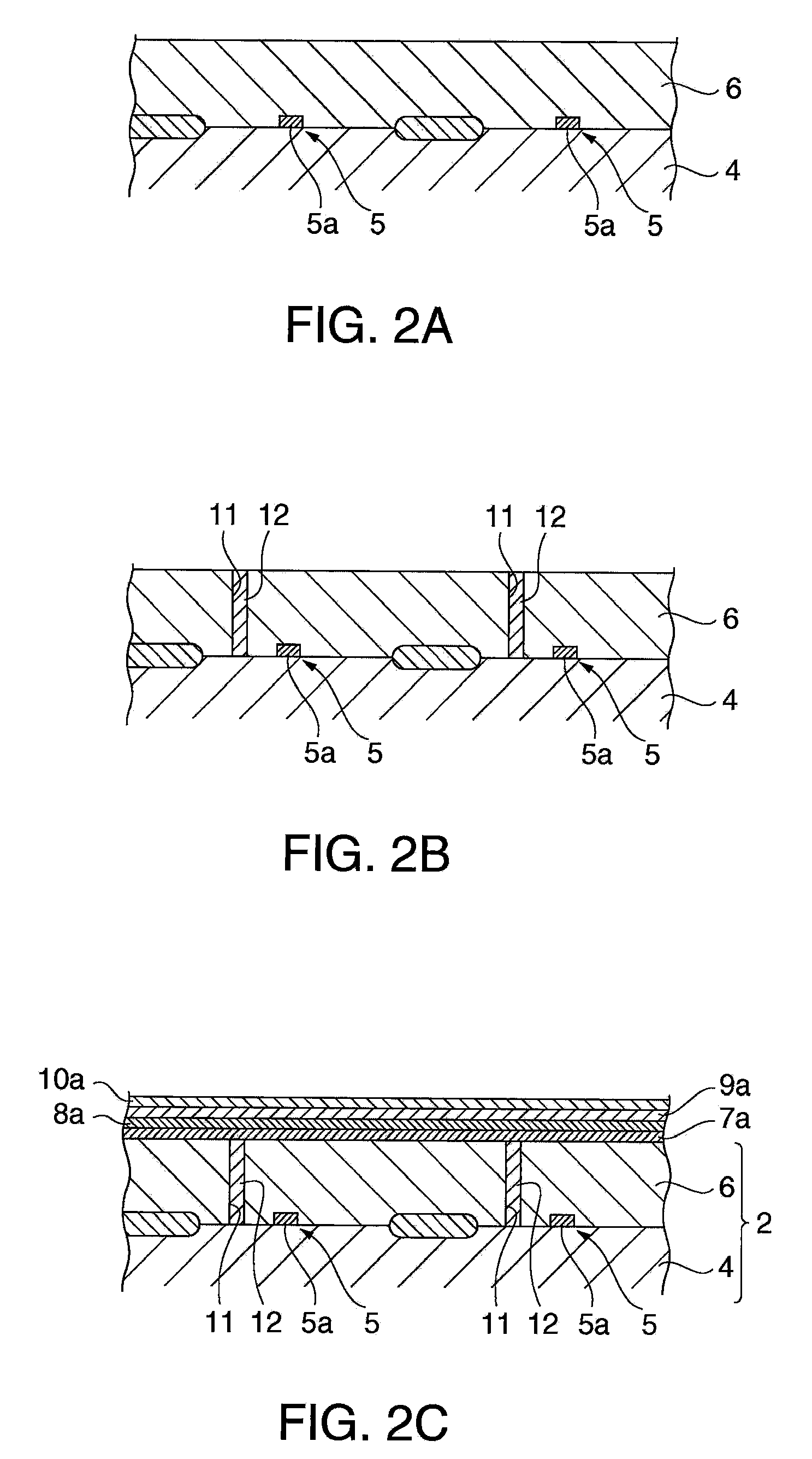
[0036]Examples of preferred embodiments of the invention are described below. First, a ferroelectric memory device in accordance with an embodiment of the invention is described. FIG. 1 is a cross-sectional view in part of a ferroelectric memory device in accordance with an embodiment of the invention. Reference numeral 1 in the figure denotes a ferroelectric memory device. The ferroelectric memory device 1 is of a stacked type having a 1T / 1C memory cell structure, and is equipped with a base substrate 2, and a plurality of ferroelectric capacitors 3 provided on the base substrate 2.

[0037]The base substrate 2 is formed from a silicon substrate (i.e., a semiconductor substrate) 4. Transistors 5 for driving the ferroelectric capacitors 4 are formed on a top surface portion of the silicon substrate 4, and a base dielectric film 6 that covers the driving transistors 5 is formed above the silicon substrate 4. Source and drain regions (not shown) and channel regions (not shown) composing ...


PUM

PropertyMeasurementUnit
temperatureaaaaaaaaaa
thicknessaaaaaaaaaa

Abstract

A method for manufacturing a ferroelectric capacitor includes the steps of: forming a ferroelectric capacitor having at least a lower electrode, a ferroelectric film and an upper electrode on a base substrate; and applying an anneal treatment to the ferroelectric capacitor in an oxygen atmosphere, wherein the step of forming the ferroelectric capacitor includes forming the ferroelectric capacitor to have a structure in which an electrode protection film composed of titanium oxide is provided on the upper electrode.

Description

[0001]The entire disclosure of Japanese Patent Application No. 2006-064010, filed Mar. 9, 2006 is expressly incorporated by reference herein.BACKGROUND[0002]1. Technical Field[0003]The present invention relates to ferroelectric memory devices having ferroelectric capacitors and methods for manufacturing the same.[0004]2. Related Art[0005]A ferroelectric memory device (FeRAM) is composed with ferroelectric capacitors, and is a nonvolatile memory that is capable of low voltage and high speed operations (see, for example, Japanese laid-open patent application JP-A-2005-277315). In such a ferroelectric memory device, its memory cell can be composed of, for example, one transistor and one capacitor (1T / 1C), whereby integration to the level of DRAM is possible. Accordingly, ferroelectric memory devices are highly expected as large capacity nonvolatile memories in recent years.[0006]For such ferroelectric memory devices, it has become an important issue to prevent deterioration of ferroele...

Claims


Application Information

Patent Timeline
Patent Type & Authority Applications(United States)
IPC IPC(8): H01L21/00
CPCH01L27/11502H01L28/55H01L27/11507H10B53/30H10B53/00
Inventor MIYAJI, MAMORU
Owner SEIKO EPSON CORP
Learn More