Light Emitting Diode Structure

Inactive Publication Date: 2007-09-06
EPISTAR CORP
View PDF5 Cites 15 Cited by
  • Summary
  • Abstract
  • Description
  • Claims
  • Application Information

AI Technical Summary

Benefits of technology

[0010] Another objective of the present invention is to provide a light emitting diode structure that can effectively reduce a resistance of a contact layer so that a light emitting efficiency can be improve.
[0011] A light emitting diode structure according to the present invention includes a contact layer of Constructive Oxide Contact Structure. The contact layer can be formed with high carrier density (i.e. high conductivity) more easily. When working with an appropriate transparent electrode, the contact layer can effectively increase a light emitting efficiency and reduce an operating voltage.
[0012] A contact layer of Constructive Oxide Contact Structure according to the present invention does not require a specific type of dopant. A transparent electrode can be formed of a material of the same conducting type as the contact layer. A junction between the transparent electrode and the contact layer can therefore be avoided.
[0013] Besides, a contact layer of Constructive Oxide Contact Structure according to the present invention has a better contact property with a transparent electrode. A transparent electrode can have a dimension roughly close to that of an active layer. A region inside the active layer through which an electric current flows can be enlarged and a light emitting region of the active layer is increased. A light emitting efficiency is thereby improved.

Problems solved by technology

In summary, a high density P-type contact layer cannot be effectively formed in a light emitting diode structure according to a prior art due to a limitation from the contact layer's physical property.
This not only increases a production cost but also reduces a yield rate of the light emitting diode.
Furthermore, a large part of an active layer of a light emitting diode structure according to a prior art is not fully exploited.
A light emitting diode structure according to a prior art thereby cannot provide a high light emitting efficiency.
A junction may be formed between the transparent electrode and the contact layer, and hence an operation of the light emitting diode may be affected.
Despite these prior efforts do increase a light emitting efficiency to some extent, a satisfactory level is not yet to achieve.

Method used


Image

  • Light Emitting Diode Structure
  • Light Emitting Diode Structure
  • Light Emitting Diode Structure

Examples


first embodiment

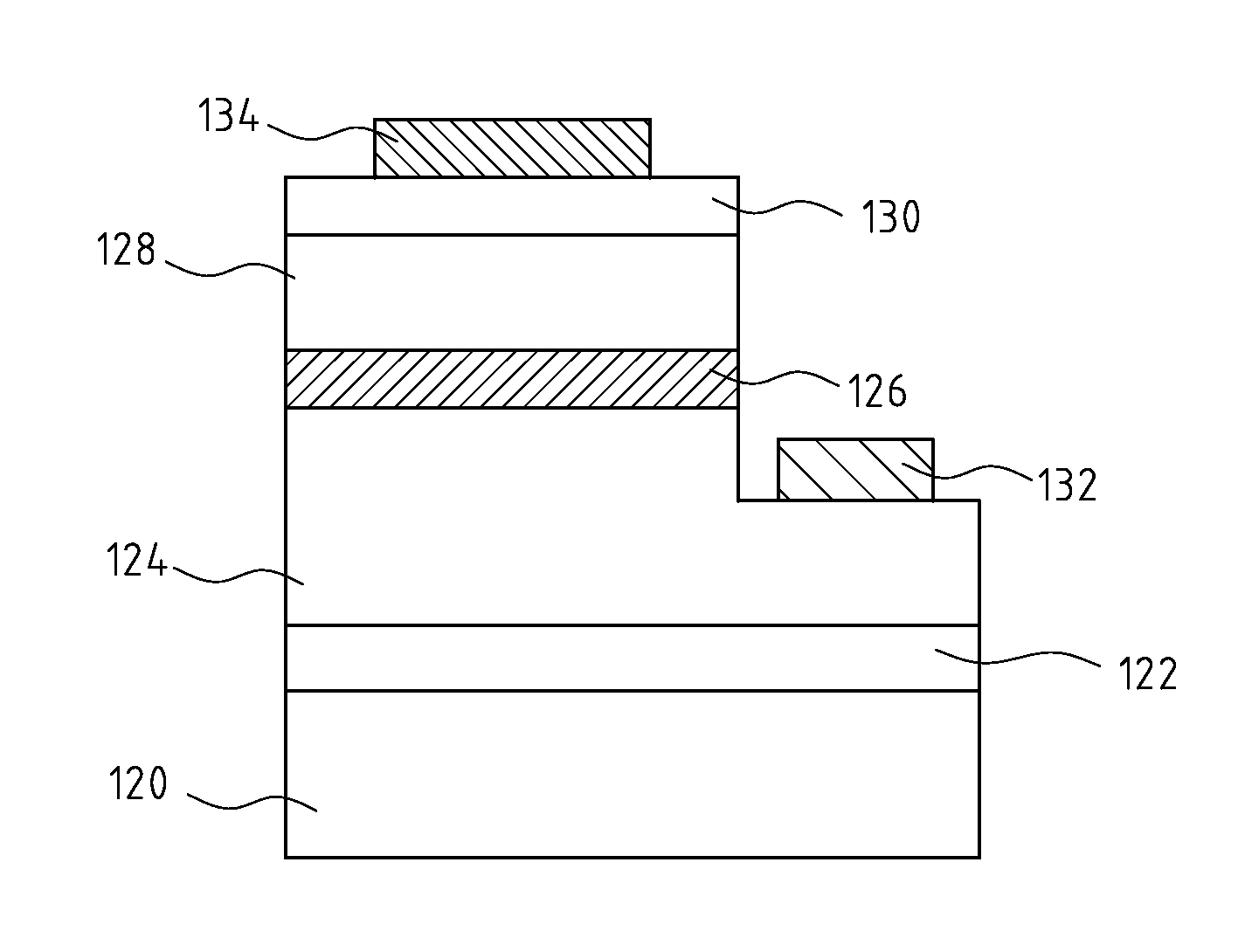
[0032]FIG. 3 is a schematic, cross-sectional diagram showing a light emitting diode structure according to the present invention. As FIG. 3 shows, the light emitting diode 100 includes a substrate 120. The substrate 120 can be made of an insulating material or a semiconducting material of a conducting type. Various kinds of materials may be used without a specific limitation. Any commonly known or unknown material that can be used to form a light emitting diode's substrate can be used in the light emitting diode structure according to the present invention. Examples of the insulating material include, but not limited to, Aluminum oxide (Al2O3, sapphire), Aluminum nitride (AlN), Gallium nitride (GaN), Spinel, Lithium Gallium oxide (LiGaO3), Lithium Aluminum oxide (LiAlO3), etc. Examples of the conducting type semiconducting material include, but not limited to, Silicon carbide (SiC), Zinc oxide (ZnO), Silicon (Si), Gallium phosphide (GaP), Gallium arsenide (GaAs), Zinc selenium (ZnSe...

second embodiment

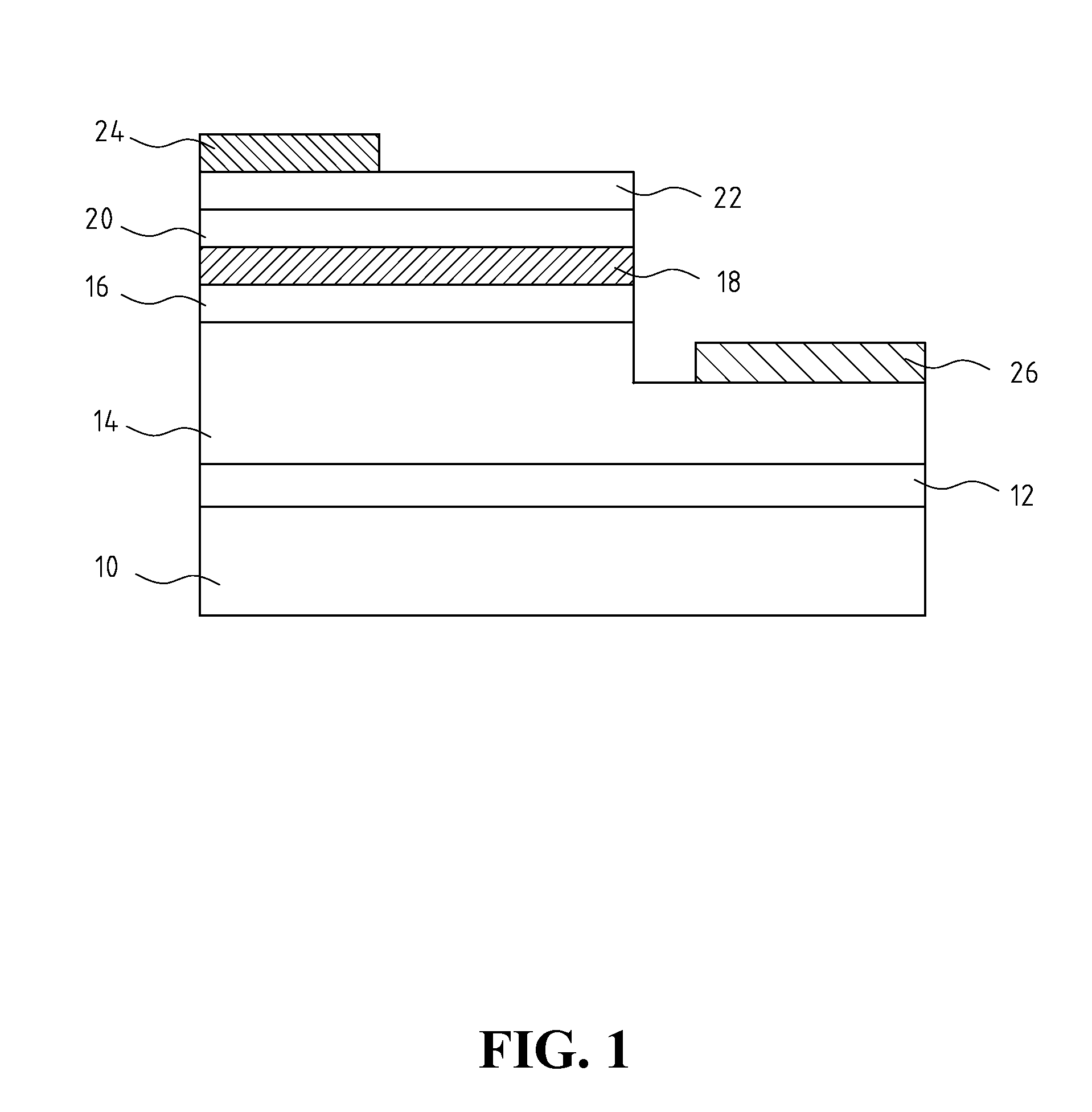
[0039] Furthermore, FIG. 5 is the schematic diagram of the band gap versus the thickness for the p-GaN layer, the InN layer, the InxGa1-xN layer, the InyGa1-yN layer, the InzGa1-zN layer, and the InN layer, sequentially stacked from bottom to top on the light emitting layer. As shown in FIG. 5, the band gaps, Eg, are decreased in the order of p-GaN layer 128>InxGa1-xN layer 130b> InzGa1-zN layer 130d> InyGa1-yN layer 130c. The band gaps of p-GaN layer 128, the InN layer 130a, the InxGa1-xN layer 130b, the InyGa1-yN layer 130c, the InxGa1-xN layer 130d, and the InN layer 130e, sequentially stacked from bottom to top on the light emitting layer, are found to be in a gradient ramp up, plateau and ramp down profile. If the band gaps of the layers stacked from bottom to top are designed in such a gradient ramp up, plateau and ramp down profile, the hole carriers can be much more easily injected from the electrode to the light emitting layer because the contact resistance can be reduced i...

third embodiment

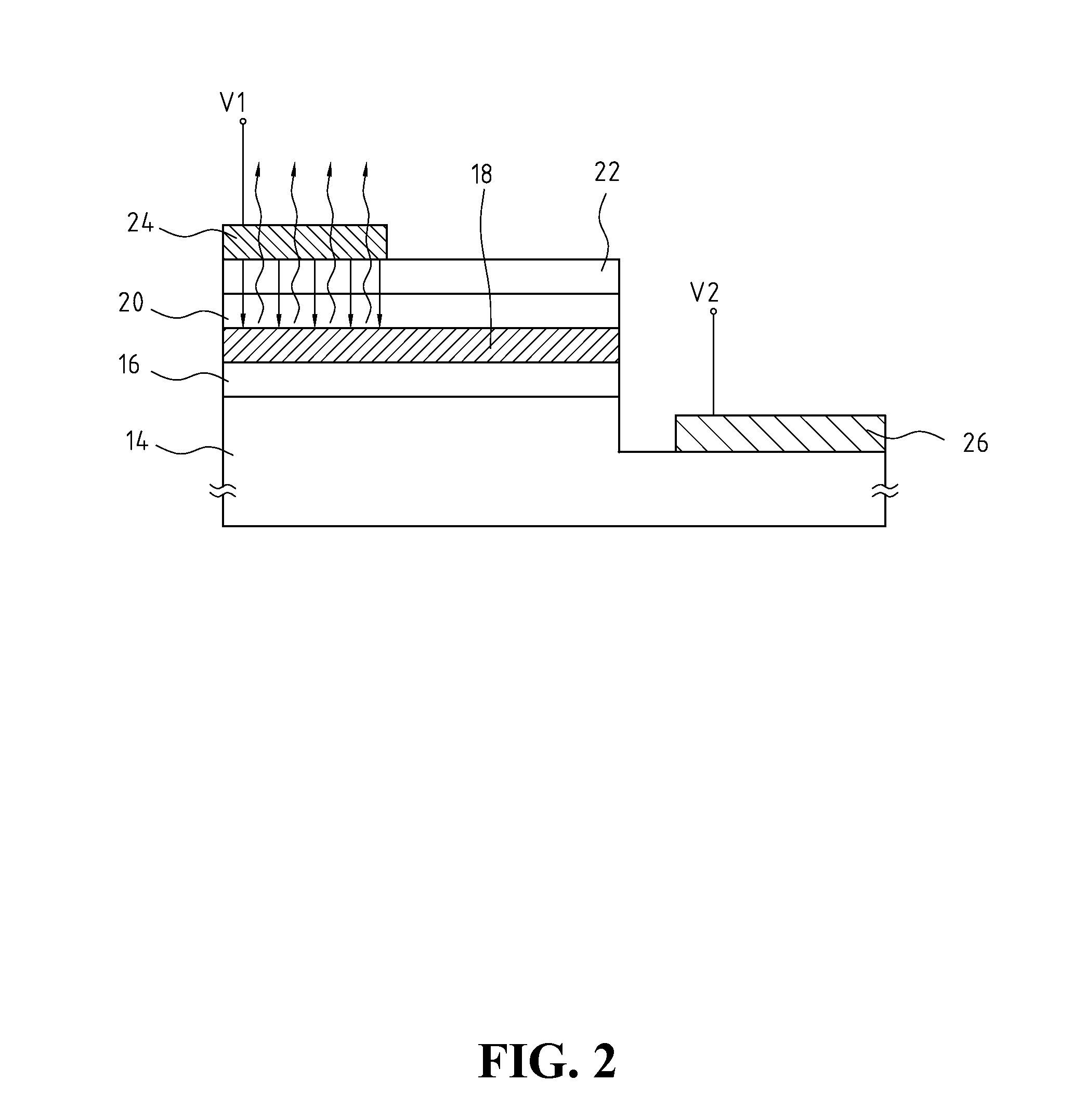
[0040]FIG. 6 is a schematic, cross-sectional diagram showing a light emitting diode structure according to the present invention. The embodiment has a similar structure as shown in FIG. 3 or 4 except that a thin film 136 of a conducting type is formed on the contact layer 130. The thin film is used for current spreading and light transparency. The thin film can also be applied in a flip chip packaging of a light emitting diode so that a heat dissipation property and an anti-electrostatic capability of the light emitting diode can be enhanced. The thin film 136 is a transparent oxide conducting layer made of an oxide thin film or an alloy, both of one, two, or more metal elements selected from a group comprising Indium (In), Tin (Sn), Zinc (Zn), Nickel (Ni), Gold (Au), Chromium (Cr), Cobalt (Co), Cadmium (Cd), Aluminum (Al), Vanadium (V), Silver (Ag), Titanium (Ti), Tungsten (W), Platinum (Pt), Palladium (Pd), Rhodium (Rh), Ruthenium (Ru), etc. The thickness of the thin film is betwe...


PUM


Abstract

Disclosed is a light emitting diode structure including a Constructive Oxide Contact Structure contact layer. The light emitting diode structure comprises a substrate, a buffer layer formed on the substrate, a lower confinement layer formed on the buffer layer, a light emitting layer formed on the lower confinement layer, an upper confinement layer formed on the light emitting layer, a Constructive Oxide Contact Structure contact layer formed on the upper confinement layer whose conducting type can be P-type, N-type, or I-type, a first electrode, and a second electrode (transparent electrode). The transparent electrode is formed on the Constructive Oxide Contact Structure contact layer as an anode of the light emitting diode. The first electrode is formed on the lower confinement layer and is spaced apart from the light emitting layer, the upper confinement layer, the contact layer, and the transparent electrode. The first electrode is used as a cathode of the light emitting diode.

Description

CROSS REFERENCE [0001] This is a continuation-in-part application for the application Ser. No. 10 / 857,682 filed on May 29, 2004.FIELD OF THE INVENTION [0002] The present invention relates to a light emitting diode structure, and more particularly, to a light emitting diode structure comprising III-V group elements and including a Constructive Oxide Contact Structure contact layer BACKGROUND OF THE INVENTION [0003] Gallium nitride (GaN) based blue light emitting diode has been industrialized on large scales worldwide since a group of Japanese researchers made a breakthrough in Gallium nitride (GaN) based extension technology in 1993. [0004] A conventional Gallium nitride (GaN) based light emitting diode structure, shown in FIG. 1, is constructed on a substrate 10 made of a material such as Al2O3. The light emitting diode 1 includes, sequentially from bottom to top, a nucleation layer 12, a N-type doped conducting buffer layer 14 made of N-type doped Gallium nitride (GaN) which makes ...

Claims


Application Information

Patent Timeline
IPC IPC(8): H01S5/00H01L29/22H01L33/02H01L33/14H01L33/32
CPCH01L33/02H01L33/32H01L33/14H01L29/2003
Inventor TSAI, TZONG-LIANGLEE, CHI-SHENHUANG, TING-KAI
Owner EPISTAR CORP
Why Eureka
Try Eureka