Organic light emitting display device with enhanced emitting property and preparation method thereof

Inactive Publication Date: 2013-06-20
SAMSUNG DISPLAY CO LTD
View PDF3 Cites 7 Cited by
  • Summary
  • Abstract
  • Description
  • Claims
  • Application Information

AI Technical Summary

Benefits of technology

The present invention is about an organic light emitting display device that can efficiently supply charges to the upper electrode, which improves light emitting efficiency. This is achieved by making the upper electrode electrically connected to power supply lines through through-holes, allowing for smooth supply of charges to the display device. This technique can be particularly effective in top-emission type organic light emitting display devices, where the cathode (lower electrode) is located on the light emitting surface. Overall, the invention provides a more efficient and effective display device with improved light emitting efficiency.

Problems solved by technology

However, when a power supply is connected to the cathode 70, i.e. the upper electrode in the above-mentioned structure, charges cannot be smoothly supplied to the cathode 70.
In particular, in a large area organic light emitting display device, it is difficult to uniformly supply charges over the entire cathode 70 having a large area.
Consequently, there is a limit in obtaining excellent light emitting characteristics.

Method used


Image

  • Organic light emitting display device with enhanced emitting property and preparation method thereof
  • Organic light emitting display device with enhanced emitting property and preparation method thereof
  • Organic light emitting display device with enhanced emitting property and preparation method thereof

Examples


Embodiment Construction

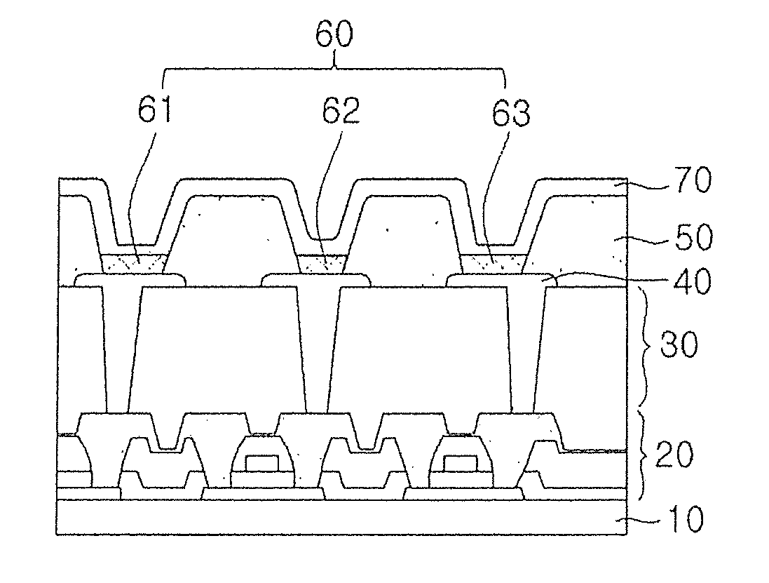
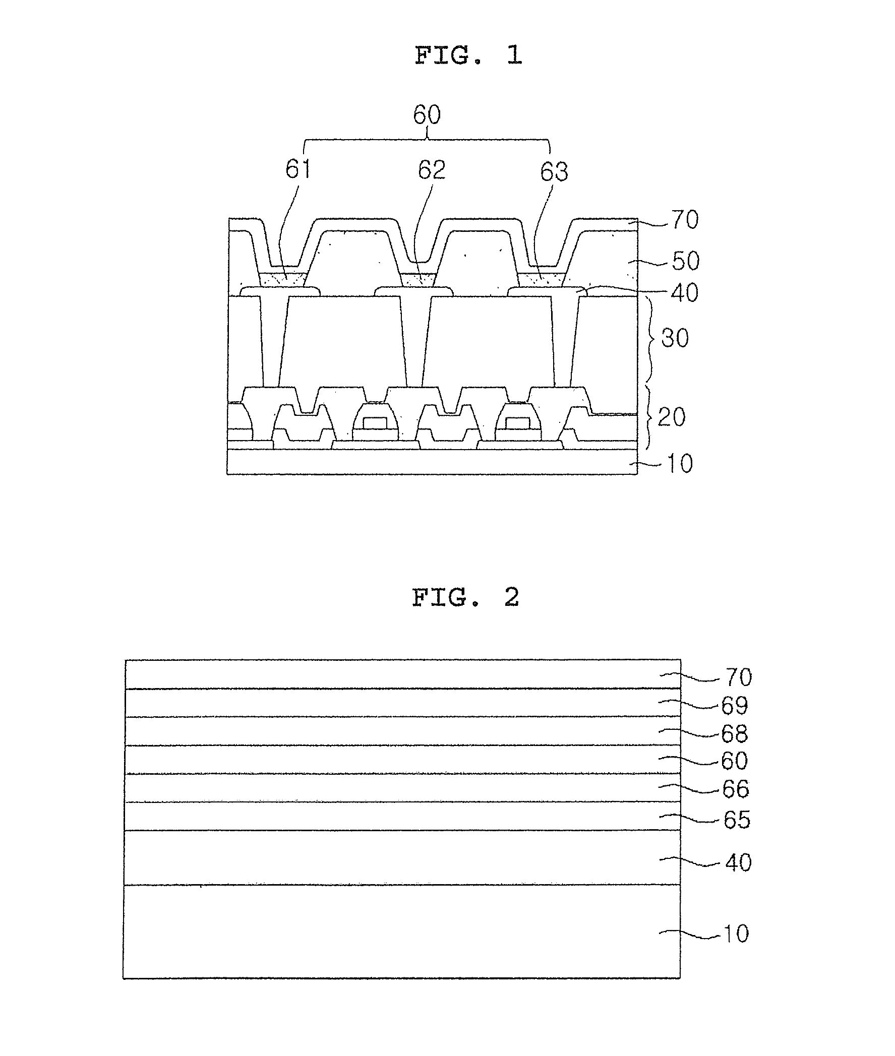
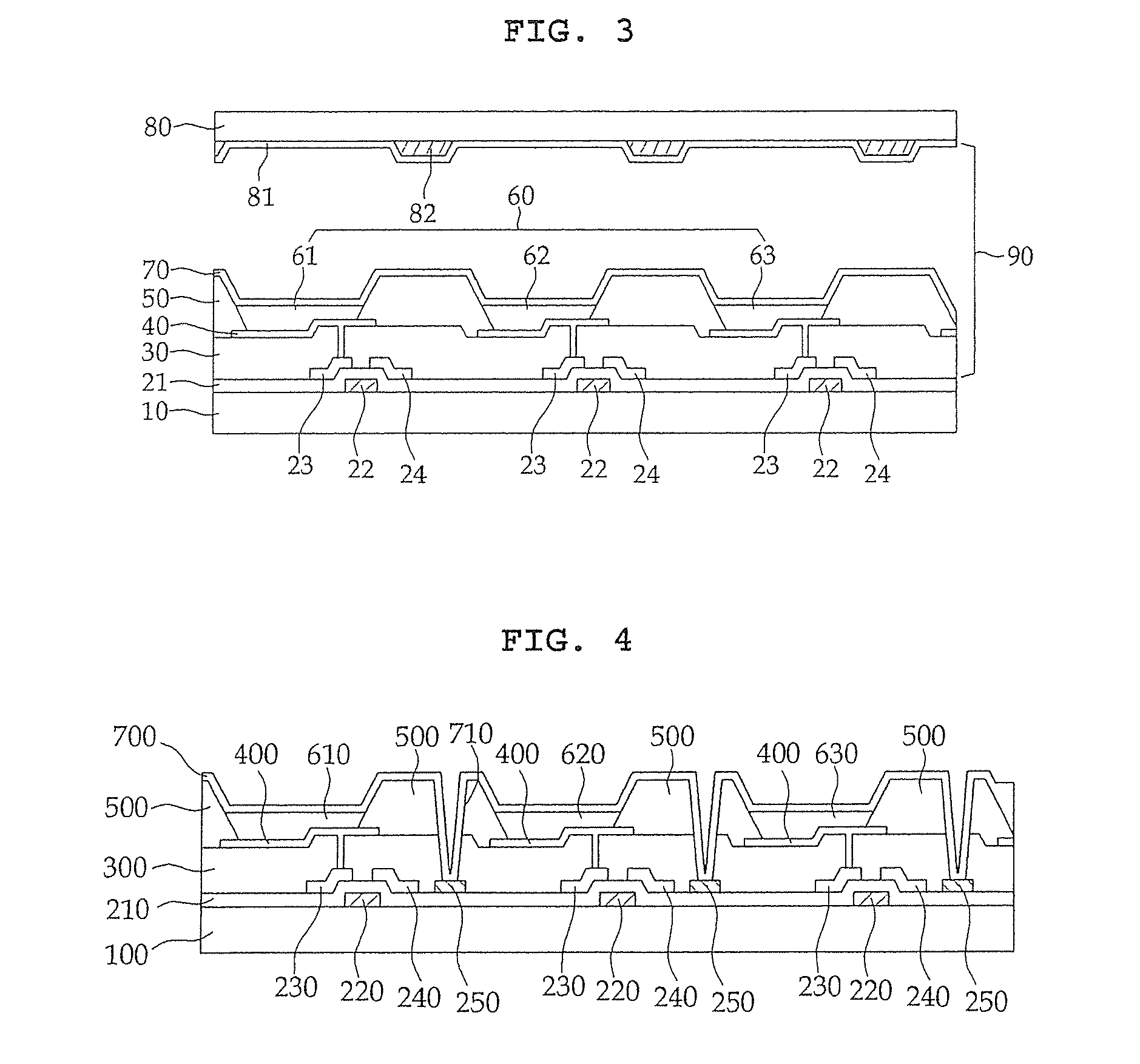
[0054]Hereinafter, exemplary embodiments of the present invention will be described in more detail with reference to the accompanying drawings. However, the scope of the present invention is not limited to the below-described embodiments and the accompanying drawings.

[0055]For reference, the elements and their shapes are schematically drawn or exaggerated in the drawings to help understanding of the present invention. In the drawings, the same / like reference numerals denote the same / like elements.

[0056]Further, when it is described that a layer or element is located on another layer or element, the layer or element may not only directly contact the other layer or element, but also one or more third layers or elements may be interposed therebetween.

[0057]FIG. 4 schematically illustrates an organic light emitting display device according to an embodiment of the present invention.

[0058]The organic light emitting display device includes a substrate 100, semiconductor layers (including g...


PUM


Abstract

An organic light emitting display device in which an upper electrode and power supply lines are connected through through-holes such that charges can be smoothly supplied to the upper electrode of the organic light emitting display device, making it possible to improve light emitting efficiency.

Description

CROSS-REFERENCE TO RELATED APPLICATION[0001]This application claims priority to and the benefit of Korean Patent Application No. 10-2011-0136042, filed on Dec. 16, 2011, in the Korean Intellectual Property Office, the entire content of which is incorporated herein by reference.BACKGROUND[0002]1. Field[0003]The following description relates to an organic light emitting display device having an improved light emitting efficiency.[0004]2. Description of the Related Art[0005]In recent years, organic light emitting display devices are being spotlighted in the field of display technology. Such an organic light emitting display device is a type of display device using light generated when electrons and holes are coupled together to form excitons, and then the excitons change from an excited state to a ground state to thereby emit light.[0006]The organic light emitting display device includes an electrode for injecting holes, an electrode for injecting electrons, and a light emitting layer,...

Claims


Application Information

Patent Timeline
IPC IPC(8): H01L27/32H01L51/56
CPCH01L27/3276H01L27/3246H10K59/122H10K59/131H10K2102/3026
Inventor LEE, WON-KYULEE, JUNE-WOOCHANG, YOUNG-JINOH, JAE-HWANJIN, SEONG-HYUN
Owner SAMSUNG DISPLAY CO LTD
Why Eureka
Try Eureka