Material composition and manufacturing method of light coupling lens for quantum dot display panel

Pending Publication Date: 2021-12-30
SHENZHEN CHINA STAR OPTOELECTRONICS SEMICON DISPLAY TECH CO LTD
View PDF2 Cites 0 Cited by
  • Summary
  • Abstract
  • Description
  • Claims
  • Application Information

AI Technical Summary

Benefits of technology

The present disclosure describes a new material composition for a light out-coupling lens that can increase the efficiency of organic light-emitting diodes (OLEDs). The lens contains quantum dots that can absorb short-wavelength components of white light emitted by OLEDs to emit red light or green light, resulting in brighter and more energy-efficient screens. The quantum dot display panel is designed to excite quantum dots to emit light, which increases color saturation and out-coupling efficiency. The quantum dots have low toxicity, corrosion, and viscosity suitable for printing. The resulting light out-coupling lens has fine light transmittance and stability.

Problems solved by technology

Therefore, OLEDs possess disadvantages of high operating temperature, energy consumption, low brightness, and limited color gamut.

Method used


Image

  • Material composition and manufacturing method of light coupling lens for quantum dot display panel
  • Material composition and manufacturing method of light coupling lens for quantum dot display panel
  • Material composition and manufacturing method of light coupling lens for quantum dot display panel

Examples


first embodiment

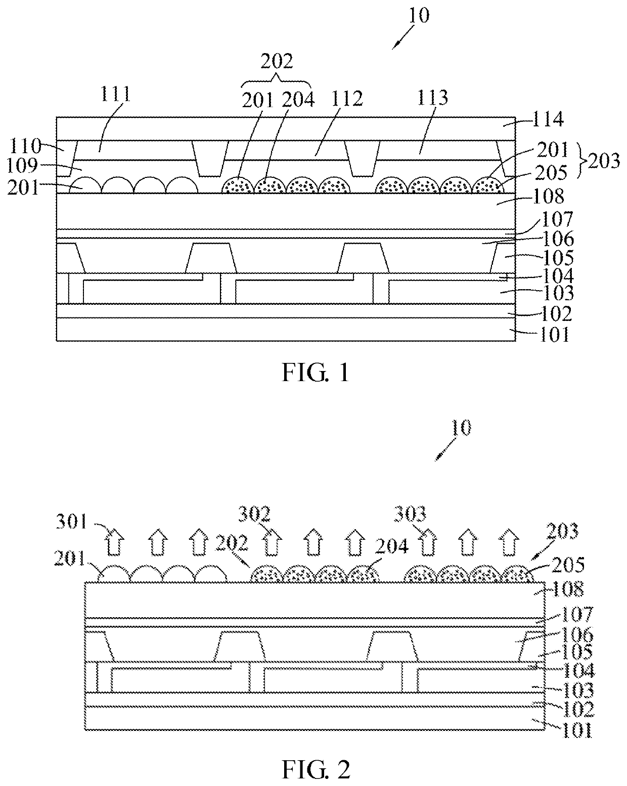
[0054]In the present disclosure, the quantum dot display panel 10 may further include a substrate 101, a thin-film transistor (TFT) array 102, a planarization layer 103, an anode 104, a pixel defining layer 105, an organic light-emitting diode (OLED) 106, a cathode 107, a thin-film encapsulation layer 108, a black matrix 110, and a cover plate 114 which are formed on the substrate 101 in sequence.

[0055]The material composition of the light out-coupling lens 201 includes trimethylolpropane tris(3-mercaptopropionate), triethyleneglycol divinyl ether, and an ultraviolet radical initiator. A molar ratio of trimethylolpropane tris(3-mercaptopropionate) to triethyleneglycol divinyl ether is 2:3. The material composition is cured by an ultraviolet light to form the light out-coupling lens.

[0056]Trimethylolpropane tris(3-mercaptopropionate) and triethyleneglycol divinyl ether can be obtained by any known manufacturing method or are commercially available.

[0057]The ultraviolet radical initia...

second embodiment

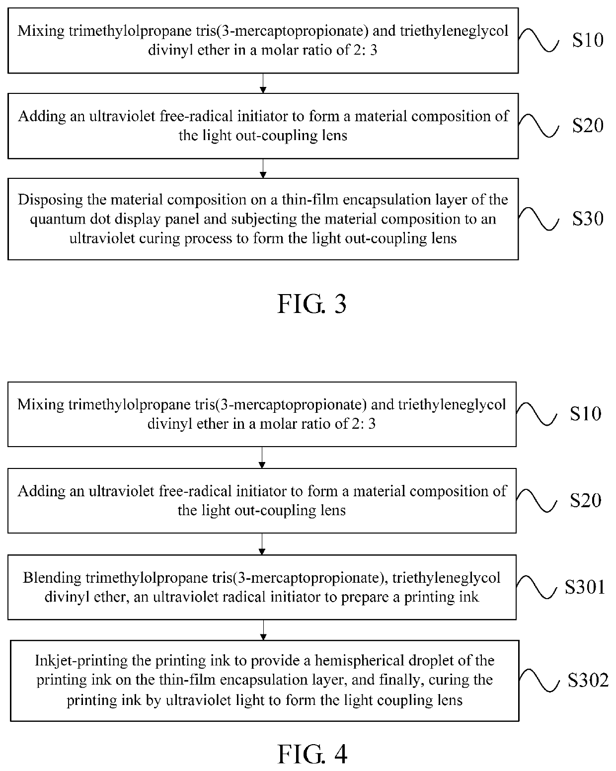
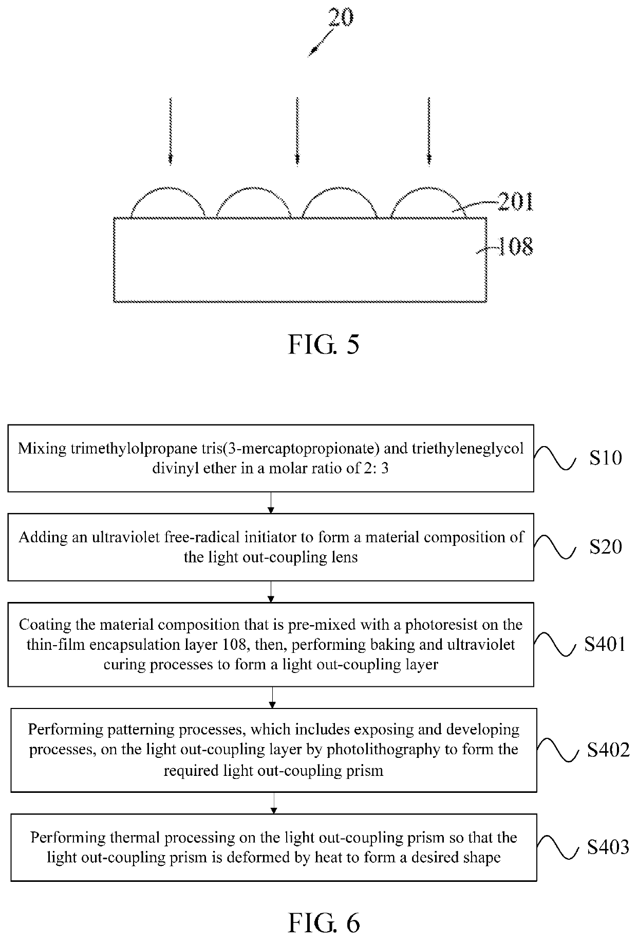
[0085]FIGS. 4-5 show the light out-coupling structure 20 of the present disclosure. The manufacturing method of the light out-coupling lens 201 includes printing (or transferring) on the thin-film encapsulation layer 108 to provide the light out-coupling composition. The manufacturing method of the light out-coupling lens 201 specifically includes:

[0086]a step S301 of blending trimethylolpropane tris(3-mercaptopropionate), triethyleneglycol divinyl ether, an ultraviolet radical initiator, (optionally) a plurality of quantum dots 204, 205 (see FIG. 2), and (optionally) a photoresist to prepare a printing ink; and

[0087]a step S302 of inkjet-printing the printing ink to provide a hemispherical droplet of the printing ink on the thin-film encapsulation layer 108, as shown in FIG. 5, and finally, curing the printing ink by ultraviolet light (arrow in FIG. 5) to form the light coupling lens 201. If a transferring process is employed, firstly, the printing ink is printed on a surface of a ...

third embodiment

[0089]FIGS. 7-9 show a light out-coupling structure 20 according to the present disclosure. The manufacturing method of the light out-coupling lens 201 includes forming an array of light out-coupling lenses on the thin-film encapsulation layer 108 after performing coating, drying, exposing, developing, heating (or by printing / transferring and curing) processes in sequence. The steps are specifically as follows:

[0090]a step S401 of coating the material composition that is pre-mixed with a photoresist and (optionally) a plurality of quantum dots 204, 205 (see FIG. 2) on the thin-film encapsulation layer 108, and, then, performing baking and ultraviolet curing processes to form a light out-coupling layer 200, as shown in FIG. 7. This step can be repeated 3 times to form light coupling output layers 200 containing red light-emitting quantum dots 204, green light-emitting quantum dots 205, without quantum dots 204, 205 at predetermined positions of the red, green, and blue sub-pixels.

[00...


PUM

PropertyMeasurementUnit
Temperatureaaaaaaaaaa
Lengthaaaaaaaaaa
Lengthaaaaaaaaaa

Abstract

A material composition and a manufacturing method of a light out-coupling lens for a quantum dot display panel are provided. The material composition includes trimethylolpropane tris(3-mercaptopropionate), triethyleneglycol divinyl ether, and an ultraviolet radical initiator. A molar ratio of trimethylolpropane tris(3-mercaptopropionate) to triethyleneglycol divinyl ether is 2:3. The material composition is cured by an ultraviolet light to form the light out-coupling lens. The manufacturing method of the light out-coupling lens includes steps of: mixing trimethylolpropane tris(3-mercaptopropionate) and triethyleneglycol divinyl ether; adding an ultraviolet free-radical initiator to form a material composition of the light out-coupling lens; disposing the material composition on a thin-film encapsulation layer of the quantum dot display panel; and subjecting the material composition to an ultraviolet curing process to form the light out-coupling lens.

Description

FIELD OF INVENTION[0001]The present application relates to the field of display technologies, and more particularly, to a material composition and a manufacturing method of a light out-coupling lens for a quantum dot display panel.BACKGROUND OF INVENTION[0002]Organic light-emitting diodes (OLEDs) possess advantages of self-emission, high contrast, and application to flexible and bended products. OLEDs are thus very promising display technologies. However, OLEDs employ white light as a base light. OLEDs require the disposition of color filters, and combinations of colors present various colors that are visible to human naked eyes. The light intensity of OLEDs depends on the magnitude of current. The greater the current, the greater the energy carried by the electrons, and the higher the brightness of the generated light. Therefore, OLEDs possess disadvantages of high operating temperature, energy consumption, low brightness, and limited color gamut.[0003]Therefore, it is necessary to...

Claims


Application Information

Patent Timeline
IPC IPC(8): C09D11/101G02B1/04H01L51/56H01L51/50H01L51/52C09D11/38C09D11/106C09D11/52B41M3/00
CPCC09D11/101G02B1/041H01L51/56H01L51/502G03F7/027C09D11/38C09D11/106C09D11/52B41M3/003H01L51/5275G02B6/4204H10K59/879H10K71/40G03F7/0007C09D11/50C09D11/322H10K59/38G03F7/0042H10K50/115H10K50/858H10K71/00
Inventor LIU, MINGWU, YUANCHUN
Owner SHENZHEN CHINA STAR OPTOELECTRONICS SEMICON DISPLAY TECH CO LTD
Why Eureka
Try Eureka