Distributed-feedback semiconductor laser, distributed-feedback semiconductor laser array, and optical module
a semiconductor laser and semiconductor laser technology, applied in semiconductor laser arrangements, semiconductor laser shapes and construction, semiconductor lasers, etc., can solve the problems of optical loss in the mirror, drive current the load on the ic is still too high, so as to achieve stable single-mode operation, short active region, and high single-mode stability
- Summary
- Abstract
- Description
- Claims
- Application Information
AI Technical Summary
Benefits of technology
Problems solved by technology
Method used
Image
Examples
first embodiment
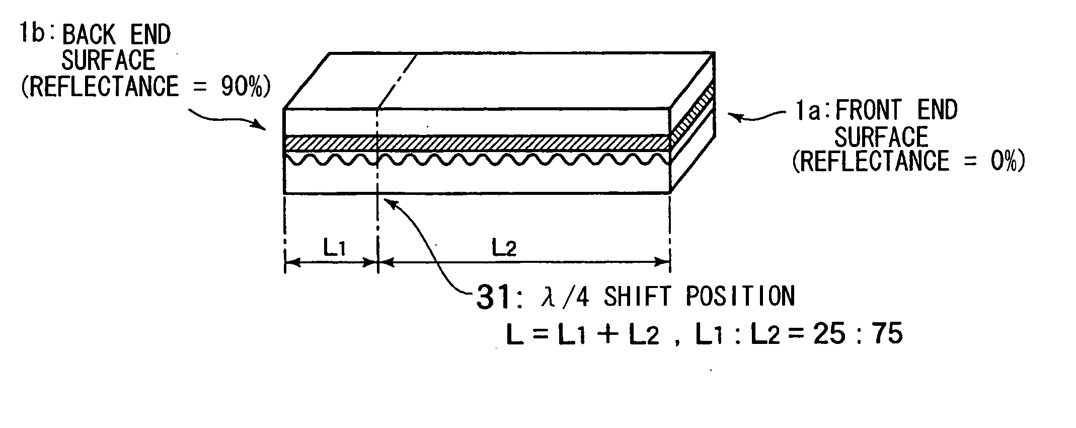
[0149] Referring to FIG. 7, a perspective view of a device 29 in which a DFB laser (distribution-feedback semiconductor laser) 1 and a monitor PD2 (another function region having a light-receiving function) are integrated in one unit is shown as a first embodiment of the present invention. Further, FIG. 8 is a schematic top plan view of the device 29 shown in FIG. 7. In FIG. 7, an Fe doped InP current blocking layer 16 is partially broken to be perspective so that the layer structure of the DFB laser 1 can be shown. Further, a SiN film 17 formed on the front end surface of the monitor PD2 is shown to be perspective in order to show the layer structure of the monitor PD2 in FIG. 7
[0150] As shown in FIGS. 7 and 8, the device 29 comprises the monolithically integrated DFB laser 1 (distribution-feedback semiconductor laser) and the monitor PD 2.
[0151] The back and forth-directional (longitudinal) length of this device 29 is, for instance, 250 μm. In other words, the total length of the...
second embodiment
[0191] In the first embodiment, an example in which the DFB laser 1 and the monitor PD2 are integrated in one unit is described, however, the present invention is not limited to this, and for instance, a device 35 that only has the DFB laser 1 can be used as shown in FIG. 15. In other words, the only difference between the device 35 relating to a second embodiment and the device 29 shown in FIG. 7 is that the device 35 does not have the monitor PD2.
[0192] In order to obtain the device 35 relating to the second embodiment shown in FIG. 15, while the waveguide mesa (not shown in the drawing) only having the region of the DFB laser 1 is formed in the etching process at the stage shown in FIG. 11, all the processes for forming the monitor PD2 are omitted.
[0193] In the case of the device 35 shown in FIG. 15, the total back and forth-directional length of the device 35 can be further reduced to, for instance, 200 μm, and a dielectric multilayer film (not shown in the drawing) can be use...
third embodiment
[0195] Further, in the aforementioned first embodiment, a device 33 into which an external reflector 3 divided into multiple parts is integrated can be created as shown in FIG. 16 by performing an etching process creating thin rectangles in an appropriate period (pitch) in the region of the monitor PD2 after the state shown in FIG. 13 has been achieved. The arrangement period for each divided part of the external reflector 3 is, for instance, 400 nm, approximately twice as much as the region of the DFB laser 1. Here, the end surface (the front and back) of each divided part of the external reflector 3 must be parallel to the back end surface 1b of the DFB laser 1 unlike the case with the monitor PD2, and the aforementioned etching process creating thin rectangles must be performed likewise.
[0196] When the external reflector 3 is integrated as shown in FIG. 16, the high-reflection film does not have to be formed on the back end surface 1b of the DFB laser 1 since the reflectance is ...
PUM
 Abstract
Description
Claims
Application Information
 - R&D
- Intellectual Property
- Life Sciences
- Materials
- Tech Scout
- Unparalleled Data Quality
- Higher Quality Content
- 60% Fewer Hallucinations
Browse by: Latest US Patents, China's latest patents, Technical Efficacy Thesaurus, Application Domain, Technology Topic, Popular Technical Reports.
© 2025 PatSnap. All rights reserved.Legal|Privacy policy|Modern Slavery Act Transparency Statement|Sitemap|About US| Contact US: help@patsnap.com


