
Method of interconnecting terminals and method for mounting semiconductor device

a technology of interconnecting terminals and mounting devices, which is applied in the direction of printed circuit assembling, printed circuit manufacturing, printed circuit aspects, etc., can solve the problems of reducing conductivity, affecting and affecting the quality of semiconductor devices, so as to reduce the amount of man-hours, the effect of increasing the yield of semiconductor devices and simplifying the supply of anisotropic electrically conductive resin

Active Publication Date: 2007-01-04
SENJU METAL IND CO LTD +1
View PDF7 Cites 90 Cited by
  • Summary
  • Abstract
  • Description
  • Claims
  • Application Information

AI Technical Summary

Benefits of technology

[0017] The present invention was made in order to solve the above-described problems of the prior art, and its object is to provide a method of interconnecting terminals which can guarantee adequate electrical connection between terminals such as opposing electrodes and which can obtain the same level of electrical resistance between terminals as with a metal connection as well as a mounting method for semiconductor devices using this connecting method.
[0041] (2) In the electrode placement step, when the anisotropic electrically conductive resin composition is supplied so as to achieve a state in which the anisotropic electrically conductive resin composition fills the entire space between the opposing semiconductor chip and circuit substrate including the space between the opposing electrode pads and circuit electrodes, supply of the anisotropic electrically conductive resin becomes simpler, the man-hours required can be greatly reduced, and metal bonding and resin bonding are simultaneously accomplished. In addition, low temperature working becomes possible when mounting a semiconductor device.

Problems solved by technology

However, in the above-described conventional electrically conductive adhesives, the electrically conductive particles contained in the electrically conductive adhesive are coated with a resin, so even if the electrically conductive particles physically contact each other due to being aligned, there is the problem that the resin which covers the electrically conductive particles causes conducting defects.
In such a case, a decrease in conductivity between the electrically conductive particles occurs, and it becomes difficult to obtain adequate reliability of the electrical connection between the opposing electrodes, and this leads to a decrease in the yield of semiconductor devices.
Therefore, conductivity on the same order as that of a metal cannot be expected.
In addition, with electronic devices which are extremely weak against static electricity, the application of an electric field from the outside thereof and arraying of the electrically conductive particles creates problems with respect to reliability of the electronic devices.

Method used


Image

  • Method of interconnecting terminals and method for mounting semiconductor device
  • Method of interconnecting terminals and method for mounting semiconductor device
  • Method of interconnecting terminals and method for mounting semiconductor device

Examples


example 1

[0101] Copper plates measuring 10 mm×10 mm×1 mm were polished with emery paper and then polished with a buff. Surface treatment was then carried out on a pair of the polished plates by deoxidizing with 6% hydrochloric acid and degreasing by ultrasonic cleaning using acetone. Then, a Sn-48In alloy as electrically conductive particles and Epicron SR-A as a resin were mixed to prepare an electrically conductive adhesive in which the content of the electrically conductive particles was 50% by volume. This electrically conductive adhesive was applied to the surface of one of the copper plates, and spacers made of stainless steel spheres were placed on the surface of this copper plate. Then, the other copper plate was placed atop the electrically conductive adhesive applied to the first copper plate, a weight of 10 g was placed atop the second copper plate, and after sitting for several seconds, the weight was removed and the electrically conductive particles within the electrically condu...

example 2

[0104] A sample after heating was obtained by the same technique as in Example 1 except for using an electrically conductive adhesive obtained by mixing a Sn-48In alloy as electrically conductive particles and Penguin Cement RD-0205 as a resin so that the content of the electrically conductive particles was 30 volume percent.

[0105] The results are shown in FIGS. 10(a) and 10(b). As shown by FIGS. 10(a) and 10(b), it can be seen that an electrically conducting path was formed by a melt of the electrically conductive particles between the pair of copper plates.

example 3

[0106] In order to investigate the surface activating effect of a resin contained in an electrically conductive adhesive, the distance between copper plates was controlled to 300 micrometers, and the molten state of electrically conductive particles was investigated.

[0107] Namely, 10 mm×10 mm×1 mm copper plates were polished by the same technique as in Example 1 and surface treatment was carried out. Then, a Sn-48In alloy (0.8454 g) as electrically conductive particles and Penguin Cement RD-0205 (0.1546 g) as a resin were mixed so that the content of electrically conductive particles was 50 volume percent to prepare an electrically conductive adhesive, and this electrically conductive adhesive was applied to the surface of one of the copper plates. In order to control the distance between the copper plates to 300 micrometers, spacers in the form of stainless steel balls with a diameter of 300 micrometers were placed on the surface of the one copper plate. Then, the other copper pla...


PUM


Abstract

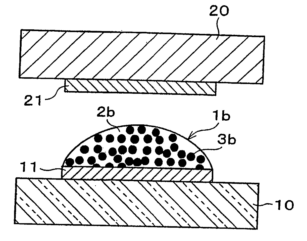
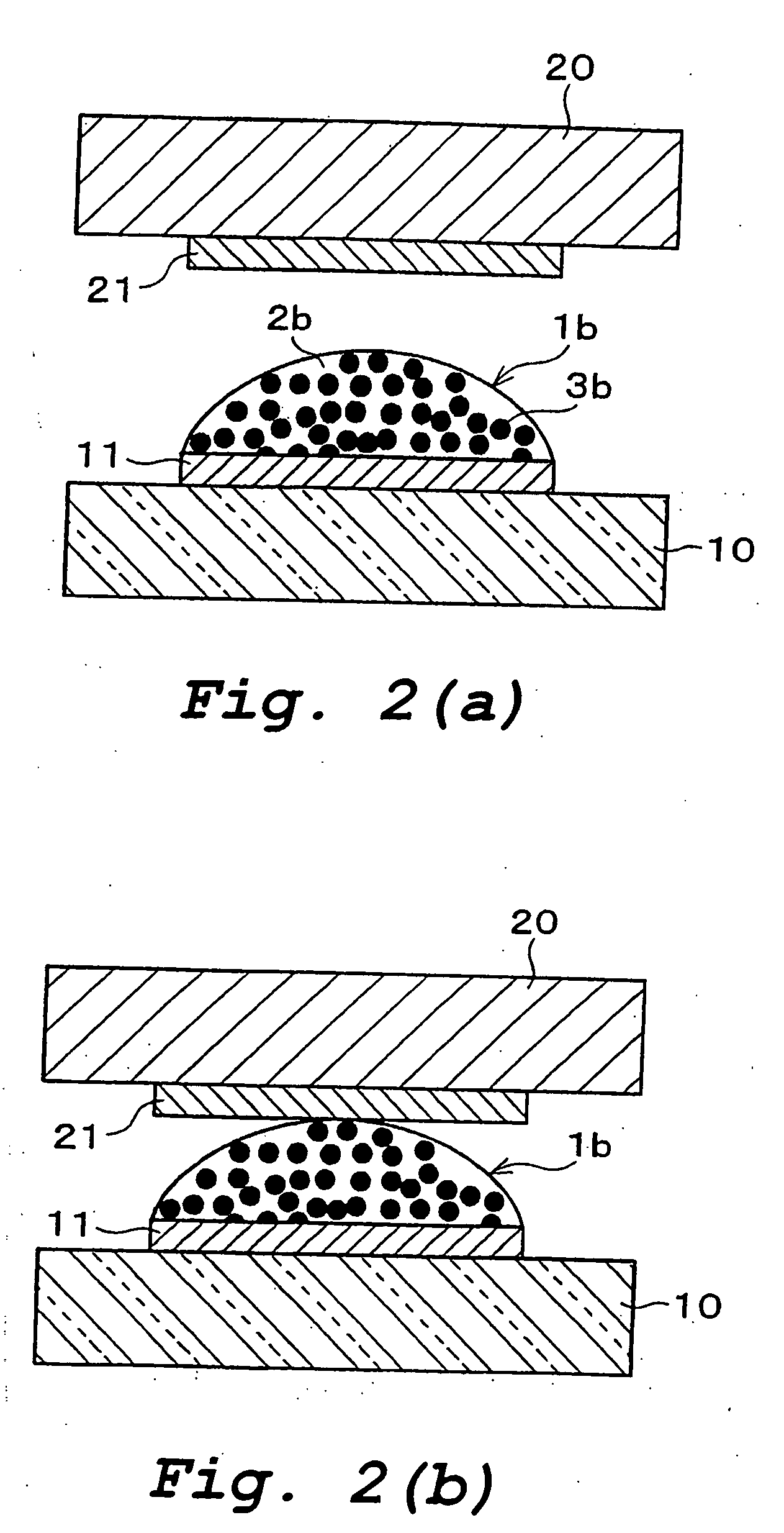
A method of interconnecting terminals so as to obtain an excellent electrical connection between terminals such as opposing electrodes and a mounting method for semiconductor devices using this connecting method are provided. Electrode pads 21 of a semiconductor chip 20 and lands 11 which are provided on a substrate 10 so as to correspond with the electrode pads 21 are placed so as to oppose each other with an electrically conductive adhesive therebetween. Then, the electrically conductive adhesive is heated to a temperature which is higher than the melting point of electrically conductive particles contained in the electrically conductive adhesive and at which a resin is not completely cured, and the electrically conductive particles are bonded to each other. Then, the semiconductor chip 20 and the substrate 10 are secured by completely curing the resin in the electrically conductive adhesive.

Description

TECHNICAL FIELD [0001] This invention relates to a method of interconnecting terminals in order to connect terminals such as electrodes provided on electronic parts such as semiconductor chips or discrete components to external terminals and to a method of mounting semiconductor devices using this connecting method. BACKGROUND ART [0002] In the field of electronics, in response to demands for higher speeds and larger capacity, smaller size and lighter weight of electronic equipment, the development of mounting technology for realizing a higher degree of integration and higher density of electronic parts such as semiconductor chips and discrete parts is being advanced. One mounting technique for such semiconductor devices which has been proposed is the flip chip mounting method using bare chips. [0003] In the flip chip mounting method, first, a plurality of electrode pads are formed on a bare chip, and bumps made of solder, gold, or the like are formed on the electrode pads. Then, in...

Claims


Application Information

Patent Timeline
IPC IPC(8): H01L23/48H01L21/00H01L21/60H05K3/32
CPCH01L24/11H01L2224/1329H01L24/83H01L2224/293H01L2224/73204H01L2224/8319H01L2924/01002H01L2924/01005H01L2924/01013H01L2924/01015H01L2924/01029H01L2924/0103H01L2924/01033H01L2924/01038H01L2924/01039H01L2924/01047H01L2924/01049H01L2924/0105H01L2924/01064H01L2924/01078H01L2924/01079H01L2924/01082H01L2924/0781H01L2924/14H05K3/321H05K2201/10674H05K2203/0425H01L2224/2919H01L2924/01006H01L2924/014H01L2924/0665H01L2224/29101H01L2924/0132H01L2924/0133H01L2924/157H01L2224/29109H01L2224/29111H01L2924/12041H01L2224/29318H01L2224/2929H01L2224/29305H01L2224/29309H01L2224/29311H01L2224/29313H01L2224/29316H01L2224/29339H01L2224/29347H01L2224/29314H01L2224/83886H01L2224/133H01L24/29H01L2924/00H01L2924/01083H01L2924/00014H01L2924/00012H01L24/05H01L2224/0554H01L2224/05568H01L2224/05573H01L2224/818H01L2224/83136H01L2224/05599H01L2224/0555H01L2224/0556
Inventor FUJIMOTO, KOZOYASUDA, KIYOKAZUKIM, JONG-MIN
Owner SENJU METAL IND CO LTD
Learn More