Method of forming a conductive contact
a technology of conductive contacts and contact surfaces, applied in the direction of semiconductor devices, semiconductor/solid-state device details, electrical apparatus, etc., can solve the problems of contact leaking into overlying materials, contact can crack, chlorine (clsub), etc., to reduce the level of undeclared components, the effect of superior results
- Summary
- Abstract
- Description
- Claims
- Application Information
AI Technical Summary
Benefits of technology
Problems solved by technology
Method used
Image
Examples
example 1
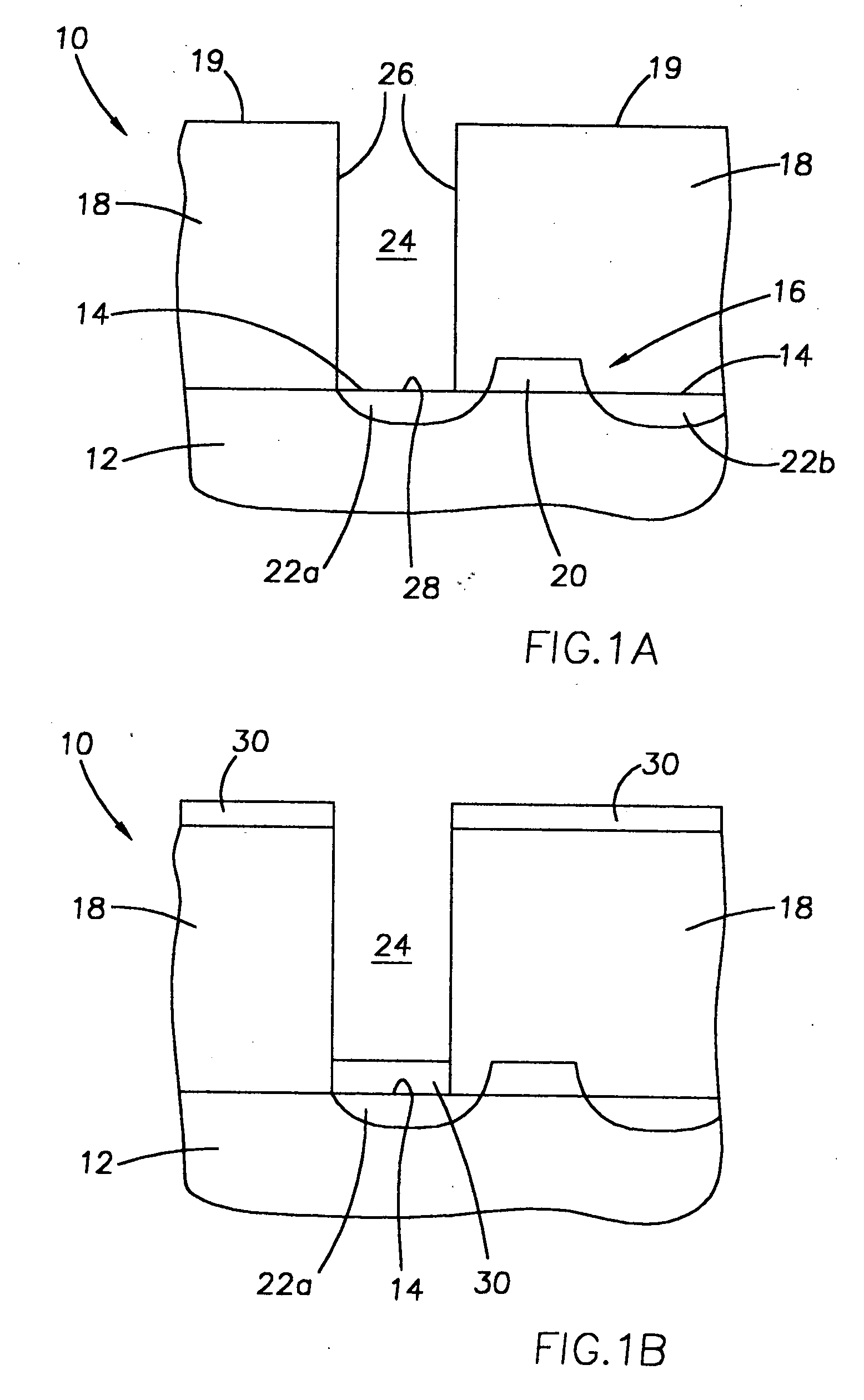
[0061] A boron-doped TiCl4-based titanium nitride (TiN) contact was formed in a high aspect ratio opening of a BPSG layer, without removal of chlorine by RTP anneal. The flow of diborane (B2H6) was varied over a range to test the change in thermal stress (Gdynes / cm2) of the boron-doped, TiCl4-based TiN contact on the BPSG insulative layer.
[0062] A wafer fragment was provided that had a silicon substrate layer and an overlying layer of BPSG. A contact opening was formed through the BPSG layer. The aspect ratio of the opening was 10:1.
[0063] The TiCl4-based TiN film was deposited by thermal CVD at a pressure of 10 Torr using a Centura system, available from Applied Materials company of Santa Clara, Calif. The precursor gases were flowed into the reactor as follows: 340 sccm TiCl4, 200 sccm NH3, 3000 sccm argon (Ar), and 2000 sccm gaseous nitrogen (N2). The diborane (B2H6) was flowed into the reactor at a rate ranging from 200 sccm to 600 sccm. Data was measured at two different temp...
example 2
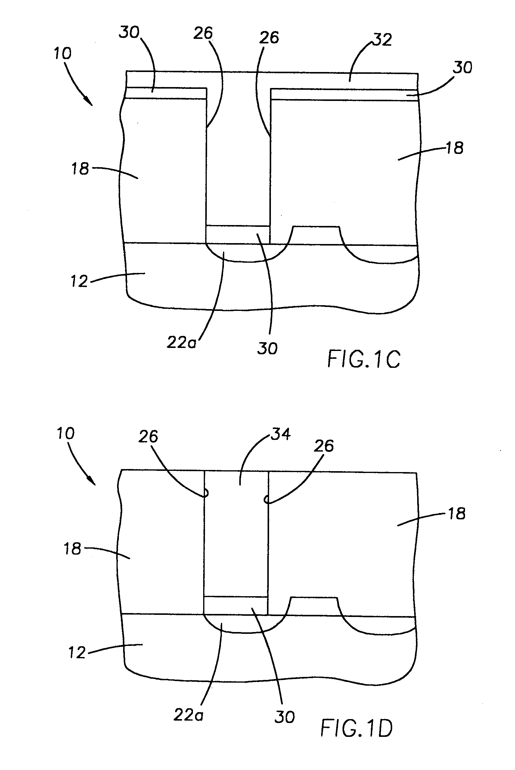
[0065] A boron-doped TiCl4-based titanium nitride (TiN) contact was formed in a high aspect ratio opening of a BPSG layer according to the method of the invention. A boron-doped TiN film was formed in a contact opening (10:1 aspect ratio) in a BPSG layer overlying a silicon substrate, as described in Example 1.
[0066] Excess titanium nitride film material was removed from the surface of the BPSG layer by conventional CMP, leaving the film material within the contact opening. The wafer was then subjected to a high temperature anneal by rapid thermal processing (RTP) in an ammonia (NH3) atmosphere at 750° C. for 25 seconds. PEELS micrographs showed differences in the chlorine (Cl2) content of the boron-doped titanium nitride material before and after the high temperature anneal.
PUM
| Property | Measurement | Unit |
|---|---|---|
| temperature | aaaaa | aaaaa |
| pressure | aaaaa | aaaaa |
| wt | aaaaa | aaaaa |
Abstract
Description
Claims
Application Information
 - R&D
- Intellectual Property
- Life Sciences
- Materials
- Tech Scout
- Unparalleled Data Quality
- Higher Quality Content
- 60% Fewer Hallucinations
Browse by: Latest US Patents, China's latest patents, Technical Efficacy Thesaurus, Application Domain, Technology Topic, Popular Technical Reports.
© 2025 PatSnap. All rights reserved.Legal|Privacy policy|Modern Slavery Act Transparency Statement|Sitemap|About US| Contact US: help@patsnap.com


