
Mask blank and process for producing and process for using the same, and mask and process for producing and process for using the same

a mask and process technology, applied in the field of mask and process for producing and processing the same, can solve the problems of image shift, deviation in the location of a pattern, and deviation of the image position, so as to achieve the effect of low generation of dus

Inactive Publication Date: 2006-10-26
KK TOSHIBA
View PDF4 Cites 18 Cited by
  • Summary
  • Abstract
  • Description
  • Claims
  • Application Information

AI Technical Summary

Benefits of technology

[0033] The invention has been developed taking the aforementioned problems into consideration, and an object thereof is to provide such a mask blank and a mask that can be applied with an electrostatic chuck, suffer no generation of dusts, and can be prevented from charging and adhesion of particles. Another object of the invention is to provide a process for producing of such a mask blank and a process for using a mask blank that enable inspection of the shape of the mask blank that measures up to required accuracy in the nanometer order, can suppress deformation of the mask blank due to formation of the electroconductive film, and can realize a flat shape with high accuracy. Still another object of the invention is to provide a mask, a process for producing the mask and a process for using the mask that use the mask blank.
[0056] As having been described, according to the above-aspects of the invention, a mask blank has a transparent electroconductive film applied thereto or an electroconductive film formed thereon, whereby such a mask blank, a process for producing the same, a process for using the same, a mask using the same, and a process for producing the mask, and a process for using the mask, that enable application of an electrostatic chuck having a sufficient retaining force, enable simultaneous inspection of the front and back surfaces of the mask blank with ultimate measuring accuracy, suffers extremely low generation of dusts, and can prevent discharge and adhesion of particles.

Problems solved by technology

In the reflection exposure system, a non-telecentric projection optical system is used on the side of the mask, and therefore, there arises a problem of image shift, in which the image location is deviated within the plane due to irregularity on the mask surface.
Furthermore, as similar to the ordinary photomasks, there is a problem of deviation in location due to elastic deformation of the mask, and deviation in location of a pattern occurs due to the weight of the mask, the stress from various thin films (such as a multilayer film, an absorbent and a buffer), the temperature and the retention.
Among these, the stress from various thin films causes a problem of deviation in pattern location due to irregularity in stress within the plane because an EUV mask has a complex film structure.
However, there are various problems on realizing the ideal flatness by the aforementioned method.
For example, a mask may not be sufficiently reformed with a chucking force of 15 kPa depending on the flat shape (warpage) of the completed mask.
In general, a particle is prevented is prevented probabilistically from being bitten by reducing the contact area of the chuck surface by several percents, but it is significantly difficult to control completely a particle on the back surface of the mask, and furthermore, the mask may not be retained with the sufficient chucking force by reducing the contact area.
In this case, not only the warping deformation of the mask cannot be reformed, but also it is difficult to retain the mask.
In this case, a vacuum chuck, which is used in the ordinary optical exposure apparatus, cannot be used.
However, taking thermal deformation due to increase in temperature upon exposure into consideration, there is such a problem that ordinary silica glass cannot satisfy the required location accuracy on thermal deformation.
Although a larger chucking force is obtained by increasing the application voltage, it is not easily practiced since it may be associated with problems in withstand voltage of dielectric breakdown and increase in leakage current.
However, the species of metallic films disclosed therein are opaque to laser light that is generally used in a mask flatness measuring apparatus, and therefore, there is such a risk that a problem occurs in a step of inspecting a mask in the production process of a mask blank described below.
In particular, such a problem may occur that sufficient inspection cannot be carried out due to shortage in measurement accuracy, so as to reduce the yield of non-defective products.
Upon resetting the substrate, the random error is increased in √2 times because of the measurement errors due to influence of difference in retaining the substrate before and after resetting and the random errors of the measurements in twice.
In this case, there is such a risk that the measurement accuracy cannot satisfy the substrate inspection specification.
As similar to the production of an ordinary photomask, it is a significant problem that adhesion of particles during the production process largely influences the yield.
A mask having a resist coated thereon is irradiated with an electron beam in the electron beam drawing step, a problem of adhesion of particles occurs due to charging when the prevention of charging up is insufficient.
It brings about such a problem that the beam does not hit on the prescribed location to deteriorate the positional accuracy.
Moreover, discharge breakdown may further occur to cause damage and deterioration of the mask material and the Cr film.
The charge up phenomenon occurs not only in the electron beam drawing step, but also in a mask production step due to ion irradiation for dry etching, which brings about such a problem that sufficient working accuracy cannot be obtained due to deterioration in etching uniformity and increase in micro loading effect.
The same problem occurs in the pattern inspection using an electron beam and repair of defects by FIB (focused ion beam).
In the production steps subsequent to the drawing step, the charge preventing film may be insufficient to avoid the problems.
Upon conveying a mask in various kinds of process apparatuses, there arises a problem of attracting particles by a charge part, in the case where charge is not sufficiently prevented from occurring.
During the process steps and in a rinsing step of the completed mask, there is also such a problem that particles are adhered to the mask, which functions as a dust collector, in the case where charge is not sufficiently prevented from occurring.
However, the molybdenum silicide oxinitride is provided between the silica glass substrate and the chromium film as a light shielding film, i.e., only on the front surface side of the substrate, and therefore, it cannot impart electroconductivity to the back surface to enable electrostatic chucking.
Furthermore, in order to apply the technique of Patent Document 5 to a mask for the 45-nm generation in the future, it is necessary that the molybdenum silicide oxinitride has a transmittance close to 100% as much as possible to excimer exposure light having a wavelength of about 193 nm, but there is such a risk that the requirement cannot be satisfied.
Accordingly, in the case where the mask is in a state where earthing is insufficient, the surface of the mask is positively charged due to disruption of the charge balance in the metallic film, which brings about such a risk that the mask functions as a dust collector.
In the case where glass as an insulating material is exposed at the peripheral part or the edge part of the mask, a uniform surface potential cannot be obtained to deteriorate the positional accuracy of patterns.
The problem occurs similarly in a process apparatus and an exposure apparatus.
However, since a mother material of a mask is silica glass as an insulating material, earthing failure occurs when the apparatus has an insufficient earthing mechanism.
For example, upon electrostatically chucking the aforementioned EUV mask, dusts are generated due to wear of the contact part of the mask and wear of the chuck upon putting on and taking off.
The problem occurs similarly upon handing by a conveying robot.
Because the problem brings about a fatal error, such as release of a film and significant generation of dusts, it is necessary that the characteristics, such as the adhesion property and the brittleness, of the electroconductive film on the back surface of the mask are carefully considered.
There is another problem that the substrate is deformed due to the internal stress of the electroconductive film itself and the thermal stress thereof upon forming the film, the film forming process and the conditions therefor are important issues as similar to the selection of film species.
(1) Problem of shortage in chucking force with glass mother material
The retaining force with an electrostatic chuck is insufficient.
The positional accuracy of patterns is deteriorated by shortage in force for reforming warpage.
The accuracy on inspecting a mask blank is insufficient.
Problems occur in the process, such as etching, SEM inspection and FIB repair.

Method used


Image

  • Mask blank and process for producing and process for using the same, and mask and process for producing and process for using the same
  • Mask blank and process for producing and process for using the same, and mask and process for producing and process for using the same
  • Mask blank and process for producing and process for using the same, and mask and process for producing and process for using the same

Examples


first embodiment

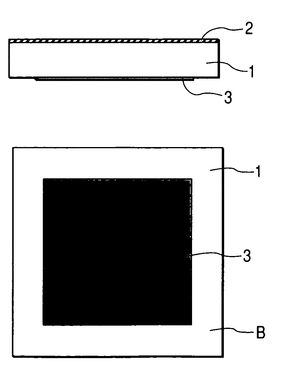
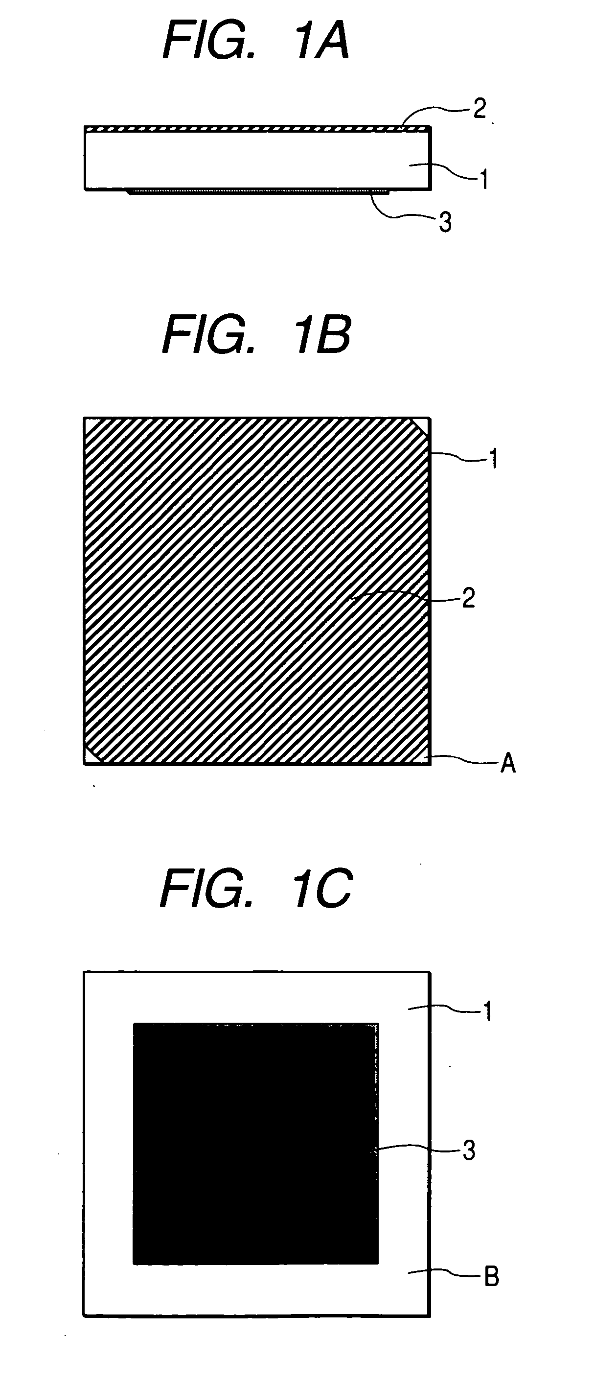
[0079] A mask blank according to a first embodiment of the invention will be described with reference to schematic constitutional figures. FIG. 1A is a cross sectional view of the mask blank, and FIGS. 1B and 1C are constitutional views thereof on the front surface and the back surface, respectively. The mask blank has the so-called 6025 outer shape specification, and a mother material 1 is fused silica glass. A light shielding film 2 formed of a Cr film having a thickness of 700 Å and a CrOx film having a thickness of 300 Å is provided on the surface. Areas A on the four corners, on which no film is formed, are used for retaining the substrate upon forming films, which are generally used as notch sections for identifying the glass substrate. For example, in SEMI P1-92 (in which the general essential matters of glass substrates for photomasks are disclosed), a substrate of silica glass has two notches facing each other on the diagonal line. An ITO film having a thickness of about 1,...

second embodiment

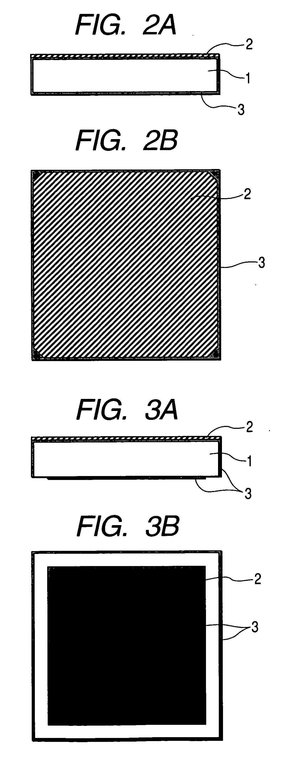
[0083] As another embodiment, FIGS. 2A and 2B show a schematic cross sectional view and a schematic front surface view of a mask blank of a second embodiment. In this embodiment, a transparent electroconductive film 3 is formed on the planes constituting all directions of the mask blank, and a light shielding film 2 is provided on the surface, on which a pattern is formed. The transparent electroconductive film is formed on the whole back surface.

third embodiment

[0084] As still another embodiment, FIGS. 3A and 3B show a schematic cross sectional view and a schematic front surface view of a mask blank of a third embodiment. In this embodiment, a transparent electroconductive film 3 is formed on the whole front surface, the whole side surface and a part of the back surface.


PUM

PropertyMeasurementUnit
Thicknessaaaaaaaaaa
Lengthaaaaaaaaaa
Transmittivityaaaaaaaaaa

Abstract

By applying a transparent electroconductive film to a mask blank or by forming an electroconductive layer by doping metallic ions thereto, such a mask blank can be provided that an electrostatic chuck having a sufficient retaining force can be applied, the front and back surfaces of the mask blank can be measured simultaneously with ultimate accuracy, generation of dusts is extremely reduced, and charge prevention and prevention of particle adhesion are enabled, and a process for producing the mask blank, a process for using the mask blank, a mask using the mask blank, a process for producing the mask, and a process for using the mask can be also provided.

Description

CROSS-REFERENCE TO RELATED APPLICATIONS [0001] This application is based on and claims the benefit of priority from the prior Japanese Patent Application No. 2005-085976, filed on Mar. 24, 2005; the entire contents of which are incorporated herein by reference. BACKGROUND OF THE INVENTION [0002] 1. Field of the Invention [0003] The present invention relates to a mask blank used in a mask for a circuit original plate used in a lithography process for producing a semiconductor device, and in particular, it relates to a structure of a mask blank, and a process for producing and process for using a mask blank. [0004] 2. Description of the Related Art [0005] In recent years, EUVL (extreme ultra violet lithography), which is a reducing reflection projection exposure technique using a soft X-ray having a wavelength of from 5 to 15 nm, is receiving attention as a next-generation lithography technique, and is being developed worldwide. In the lithography technique, a mask, an illumination op...

Claims


Application Information

Patent Timeline
IPC IPC(8): B32B9/00B32B17/10B32B17/06G03F1/00G03F1/40G03F1/50G03F1/68H01L21/027
CPCC03C17/36C03C17/3649C03C17/3652C03C17/3655C03C17/3665C03C17/3668G03F7/70708C03C2218/10C03C2218/31C03C2218/32C03C2218/34C03C2218/365G03F1/14C03C23/0055G03F1/38Y10T428/31616
Inventor MITSUI, SOICHIRO
Owner KK TOSHIBA
Learn More