Capacitor layer forming material, method of manufacturing a composite foil used where manufacturing the same, and print wiring board having a circuit where a capacitor is embedded, obtained by using the same

a technology of capacitor layer and forming material, which is applied in the direction of printed capacitor incorporation, fixed capacitor details, fixed capacitors, etc., can solve the problems of reducing the thickness of the capacitor layer forming material itself, limiting the improvement of the surface area of the capacitor, and unable to increase the capacitor electrode area beyond a certain level, etc., to achieve high adhesion and withstand expansion

Inactive Publication Date: 2006-04-27
MITSUI MINING & SMELTING CO LTD
View PDF0 Cites 4 Cited by
  • Summary
  • Abstract
  • Description
  • Claims
  • Application Information

AI Technical Summary

Benefits of technology

[0074] The capacitor layer forming material of the present invention is provided with the highly heat-resistant composite foil for the second electroconductive layer which constitutes the lower electrode. Therefore, the capacitor circuit of the above material will retain its shape and will withstand expansion and contraction induced by heat from the surrounding materials, even when exposed cyclically to hot pressing carried out at 300 to 400° C., used for production of a multilayer printed wiring board with a substrate of Teflon or liquid-crystal polymer. Moreover, by selecting the type and structure of the layers of the dissimilar metals in the composite foil in accordance with the dielectric layer type, high adhesivness of the two is achieved. Thus, by incorporating a capacitor circuit composed of the herein described capacitor layer forming material into a printed circuit board, the sought advantageous qualities described above are found. Finally, manufacture of the composite foil for production of the capacitor layer forming material of the present invention can be performed by plating copper foil with one or more heat-resistant dissimilar metal layers, a common procedure.

Problems solved by technology

It is however apparent that a capacitor has a limit in improvement for surface area (A), because increasing capacitor electrode area beyond a certain level is impossible in a printed wiring board area of given size.
Decreasing thickness of the dielectric layer, however, will lead to decreased thickness of the capacitor layer forming material itself.
Because the decreased thickness increases the fragility of the material, undesirable increases in breakage occur.
Similarly, when a sol-gel process is employed to produce the dielectric layer on a metallic foil, the resulting product becomes brittle through oxidation as a result of heating the sol-gel film to 600° C., as disclosed by Patent Document 4.
In another example, a capacitor having a lower electrode coated with a nickel / phosphorus alloy layer may involve disadvantages resulting from possible delamination of the electrode and alloy layer from each other due to insufficient adhesion between them.
A delaminated capacitor may fail to satisfy design properties due to its variable capacitance.
The delaminated portion may serve as an origin of further delamination of another portion in the printed wiring board, causing other problems such as interlayer delamination in the presence of thermal shock resulting from soldering reflow or the like.
Collectively, these problems damage product life and limit usefulness of the product.

Method used


Image

  • Capacitor layer forming material, method of manufacturing a composite foil used where manufacturing the same, and print wiring board having a circuit where a capacitor is embedded, obtained by using the same
  • Capacitor layer forming material, method of manufacturing a composite foil used where manufacturing the same, and print wiring board having a circuit where a capacitor is embedded, obtained by using the same
  • Capacitor layer forming material, method of manufacturing a composite foil used where manufacturing the same, and print wiring board having a circuit where a capacitor is embedded, obtained by using the same

Examples


example 1

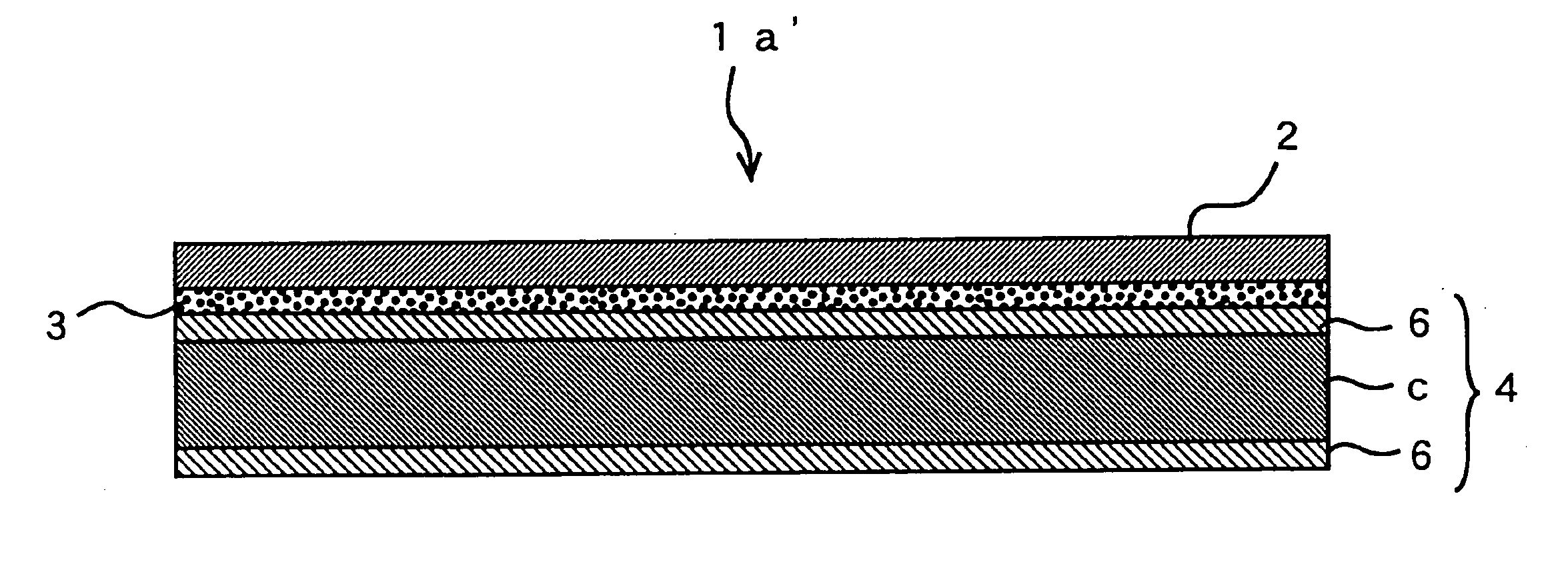
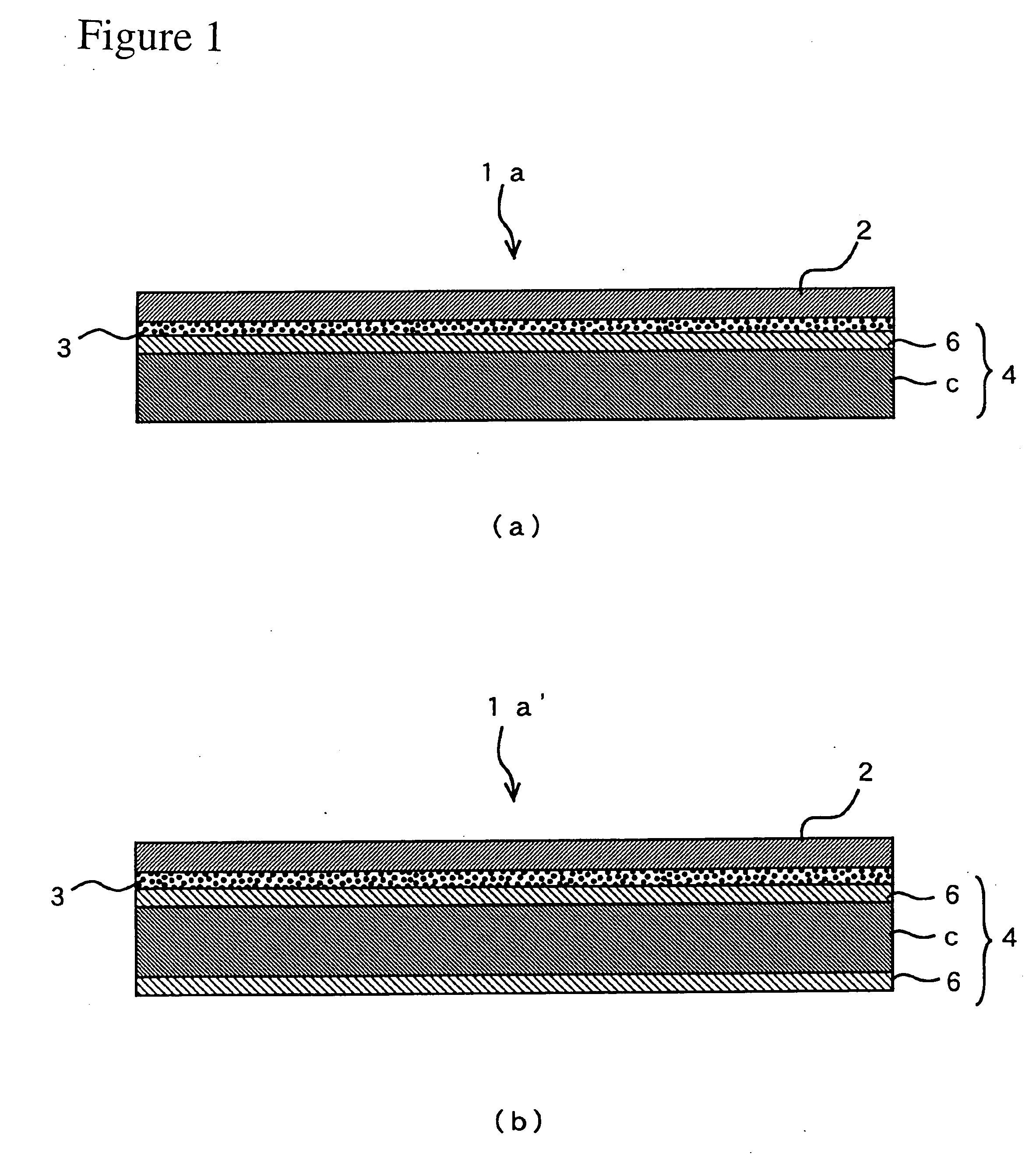
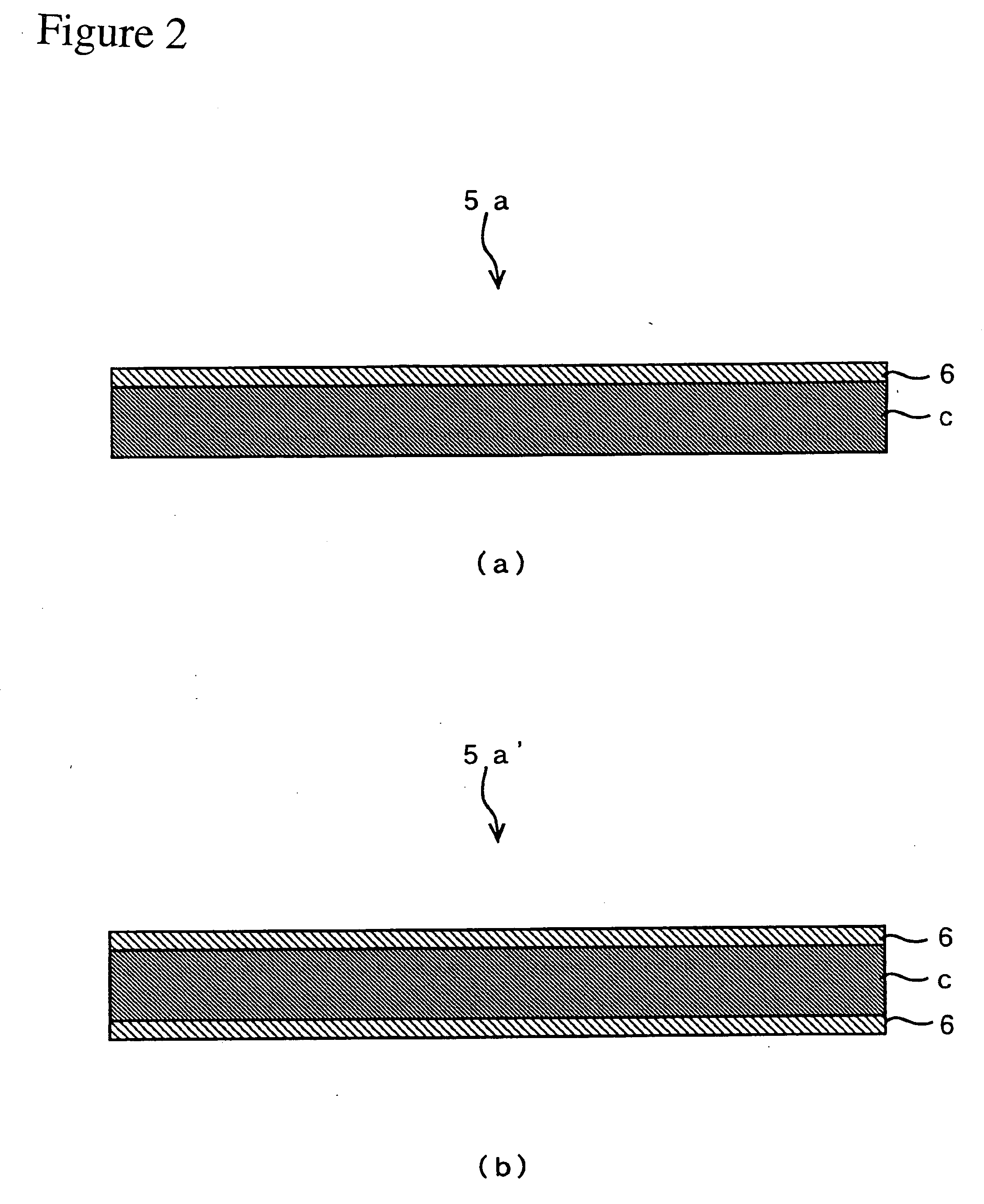
[0113] Example 1 produced the first composite foil provided with a plated hard nickel layer, capacitor layer forming material using the first composite foil, and printed wiring board with a built-in capacitor circuit.

[0114] An electrolytic copper foil (thickness: 12 μm, VLP foil, Mitsui Mining & Smelting) was dipped in an electrolytic plating solution of hard nickel of the following composition, and plated under the following conditions to form a plated hard nickel layer on the foil, to a thickness of 2 μm on the glossy surface and to a thickness equivalent to 3 μm on the rough surface. The resulting first composite foil had a total thickness of 17.5 μm. Thickness of the dissimilar metal layer, described in this specification, means the value based on the coating weight for forming the layer of given thickness on a flat surface by plating. Thickness of the actually produced composite foil means gauge thickness. The same applies to the composite foils produced in all Examples and Co...

example 2

[0127] Example 2 produced the first composite foil provided with a cobalt layer, capacitor layer forming material using the first composite foil, and printed wiring board with a built-in capacitor circuit.

[0128] An electrolytic copper foil (thickness: 12 μm, VLP foil, Mitsui Mining & Smelting) was dipped in an electrolytic plating solution of cobalt of the following composition, and plated under the following conditions to form a plated cobalt layer on the foil, to a thickness of 2 μm on the glossy surface and to a thickness equivalent to 3 μm on the rough surface. The resulting first composite foil had a total thickness of 17.8 μm.

[0129] (Cobalt Plating Solution Composition)

CoSO4.7H2O180g / LH3BO330g / LCoagulant0.1g / L

(Acrylamide-based polymer, PN-171 ®, Kurita Kogyo)

[0130] (Plating Conditions)

Solution temperature35° C.pH4Current density10 A / dm2StirringAdopted

[0131] The second composite foil produced above was analyzed for its tensile strength and elongation under the normal sta...

example 3

[0133] Example 3 produced the first composite foil provided with a nickel / cobalt alloy layer, capacitor layer forming material using the first composite foil, and printed wiring board with a built-in capacitor circuit.

[0134] An electrolytic copper foil (thickness: 12 μm, VLP foil, Mitsui Mining & Smelting) was dipped in an electrolytic plating solution of nickel / cobalt alloy of the following composition, and plated under the following conditions to form a plated nickel / cobalt alloy layer on the foil, to a thickness of 2 μm on the glossy surface and to a thickness equivalent to 3 μm on the rough surface. The resulting first composite foil had a total thickness of 17.2 μm.

[0135] (Nickel / Cobalt Electrolytic Plating Solution Composition)

NiSO4.6H2O200 g / L NiCl2.6H2O36 g / LCoSO4.7H2O12 g / LH3BO330 g / LHCOONa45 g / L

[0136] (Plating Conditions)

Solution temperature45° C.pH4Current density10 A / dm2StirringAdopted

[0137] The third composite foil produced above was analyzed for its tensile stren...


PUM


Abstract

It is an object to provide a capacitor layer forming material useful for a printed wiring board with a substrate of fluorine resin, liquid-crystal polymer or the like, which is fabricated by hot-pressing at 300 to 400° C., and showing no deterioration in strength after the hot-pressing. In order to achieve the object, the capacitor layer forming material, comprising a first electroconductive layer used for forming an upper electrode and second electroconductive layer used for forming a lower electrode with a dielectric layer in-between for a printed wiring board, has the second electroconductive layer made of a composite foil comprising a copper layer coated with one or more layers of, plated hard nickel, plated cobalt and plated nickel/cobalt alloy.

Description

BACKGROUND OF THE INVENTION [0001] 1. Field of the Invention [0002] The present invention relates to a material for forming a capacitor layer to be built in a printed wiring board, method for producing a composite foil used for forming the capacitor layer forming material, and printed wiring board provided with a built-in capacitor circuit in which the same material is used. [0003] 2. Description of the Related Art [0004] A multilayer printed wiring board provided with a built-in capacitor circuit (element) uses one or more insulation layers positioned in the inner layer for the board as dielectric layer(s). An inner circuit positioned on each side of a dielectric layer includes a capacitor circuit with an upper and lower electrodes facing each other, as disclosed by Patent Document 1 (JP-A 2003-105205). This capacitor works as a built-in capacitor. The capacitor circuit is generally formed with a capacitor layer forming material having a layered structure of first electroconductive...

Claims


Application Information

Patent Timeline
Patent Type & Authority Applications(United States)
IPC IPC(8): H01G4/005
CPCH05K1/162H05K3/384H05K2201/0355H05K2201/09309H05K2201/09509H05K2203/0723
Inventor SAKATA, TOMOHIROTANIGUCHI, KAZUKODOBASHI, MAKOTO
Owner MITSUI MINING & SMELTING CO LTD
Why Eureka
Try Eureka