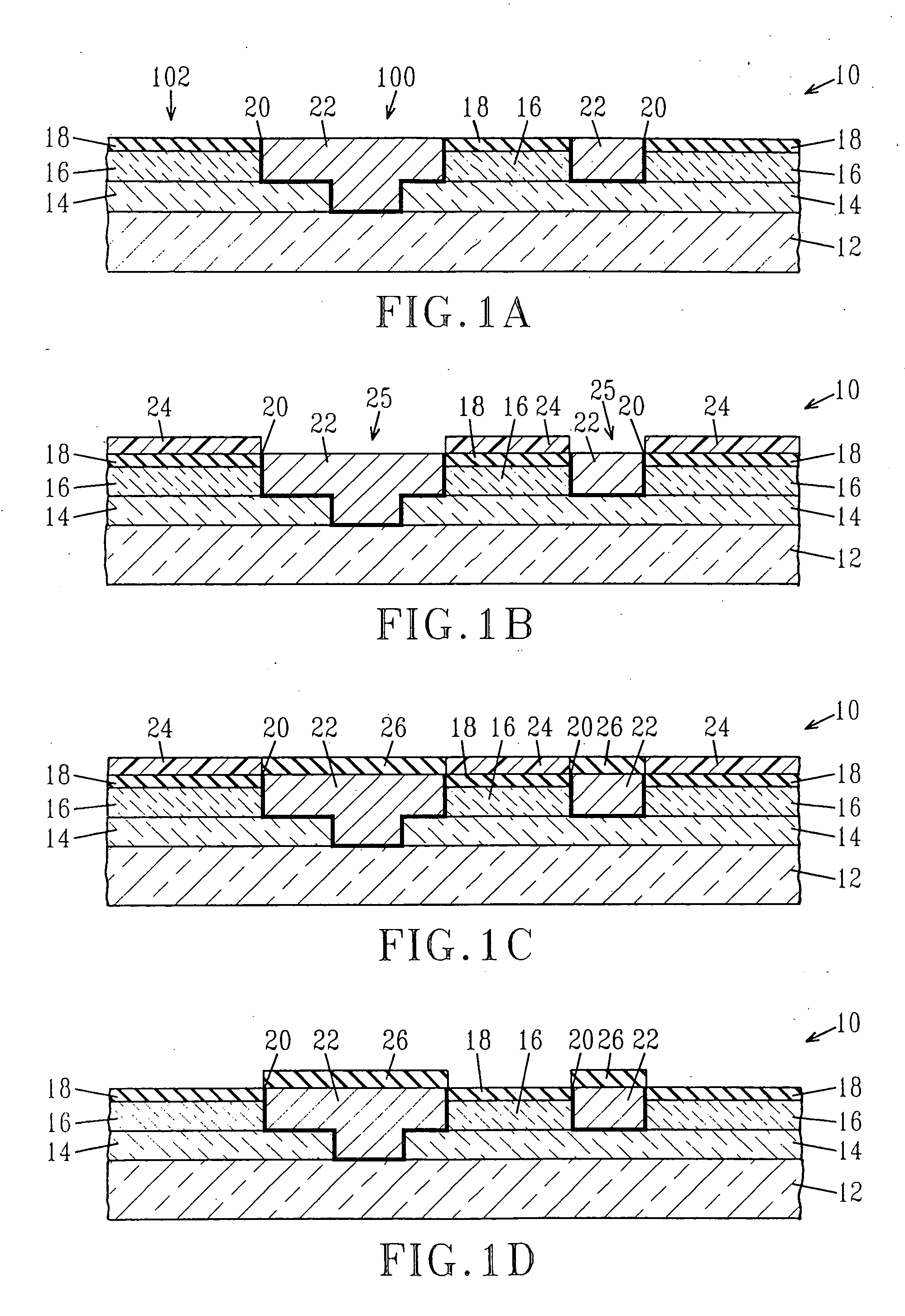
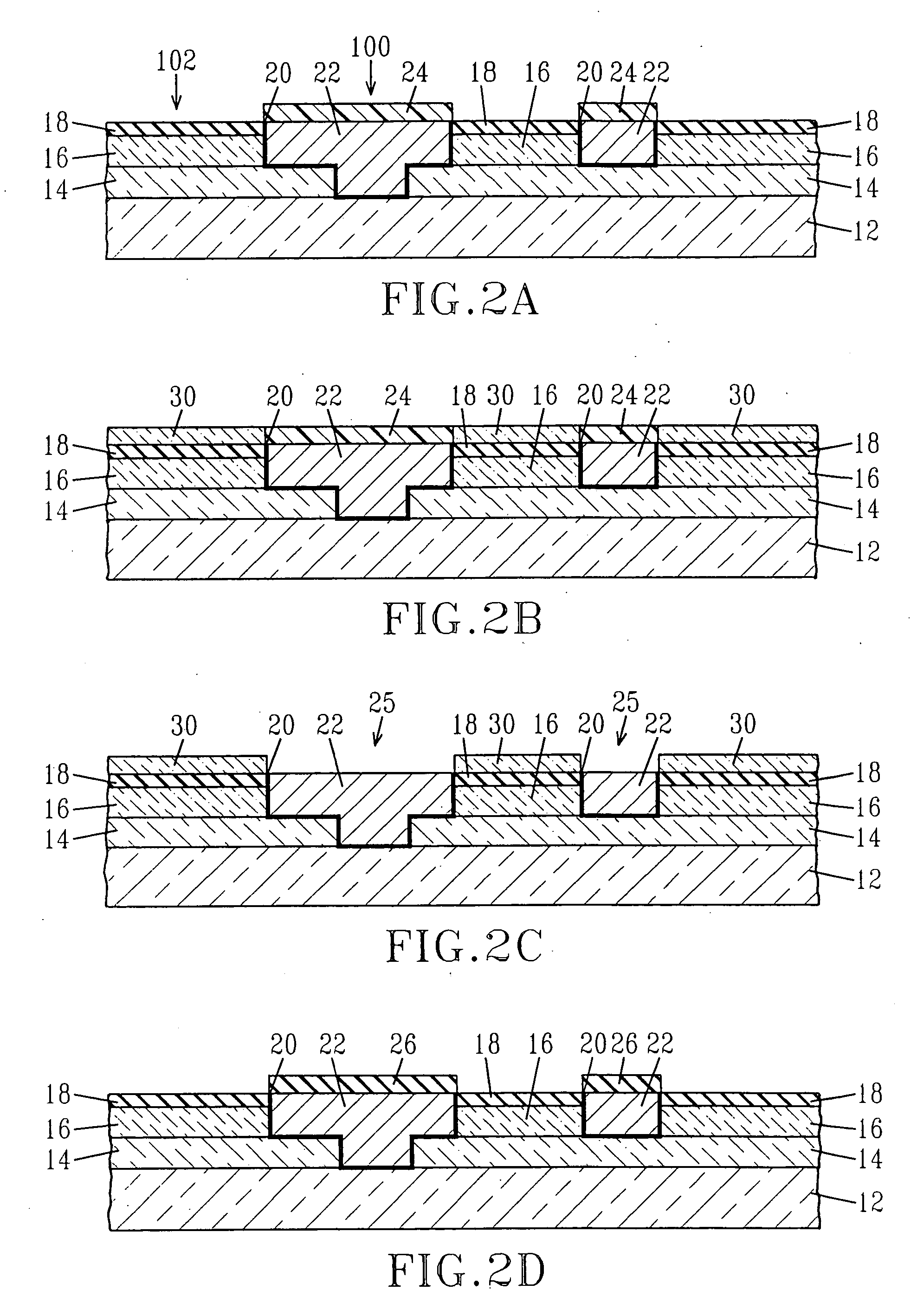
[0006] Consequently, the pattern generated in the masking material is self-aligned to the substrate upon which it is placed. The method of the present invention can apply to any technology or application involving a heterogeneous substrate including, for example, interconnect structures for high speed microprocessors,
application specific integrated circuits (ASICs), memory storage, displays, hi-
throughput screening methods, such as a
lab on a chip, microfabricated fluidic devices, etc. The utility of the inventive method stems from a simple and robust means in which the replication of a
patterned substrate to generate a self-aligned
mask can be performed, circumventing the requirement for difficult and error prone methods, such as alignment of a
lithography mask relative to pre-
patterned substrate.
[0007] Thus, the present invention provides an extremely advantageous alternative to the prior art techniques. The present invention provides a means to replicate a pattern on a pre-patterned substrate in such as manner as to act as a mask. For example, the effective
dielectric constant of an interconnect structure can be reduced by the use of a process where
layers are selectively placed upon a capped interconnect structure and used to remove the high-k dielectric cap between the
metal lines. Additionally, in the opposite tone, for which self-alignment is on the dielectric / hard-mask surfaces of an interconnect structure, the
resist, can then be used as a mask for subsequent deposition of other
layers that serve as
diffusion barriers to
copper, barriers to
oxygen and / or water
permeation, layers which reduce the
electromigration attributes of the metal lines, and seed layers. By using these processes, the mask can be self-aligned such that
overlay processes are not required to define the features. Both tones of masking (i.e., positive and negative) can be beneficial depending on subsequent
processing requirements. An additional benefit of the present invention is that neither an expensive
lithography mask, nor an expensive lithography
system is required. Rather, a simple
exposure tool that is able to generate a
blanket exposure can be utilized. In some embodiments of the present invention, it may be beneficial to have an exposure
system that is monochromatic.
[0008] Thus, in the example of integrated circuits, the use of the self-aligned masks allows a unique process in which the effective dielectric constant between metal lines can be reduced through selective application of various materials to the metal lines or as a selective mask for removing high-k dielectric material between the metal lines. The term “high-k dielectric” is used in the present invention to denote an insulator material that has a dielectric constant, k, greater than 3.0 preferably greater than 7.0. This is of great importance in maximizing the propagation speed of interconnect signals and ultimately provides faster overall
circuit performance. Furthermore, the present invention leads to a higher level of protection as well as reliability of interconnect structures and reduced
processing costs relative to comparable lithographic processes utilizing overlay strategies.
[0013] In one embodiment, the developed patterned masking material may be exposed to a dry etch process to
expose either a first region or a second region on the substrate. In another embodiment, the masking material has a thickness equal to a minima or maxima in a plot of reflectivity versus
resist film thickness for one or more of the surfaces of interest. In yet another embodiment of the present invention, the masking material has a thickness that maximizes the difference in the thickness of the masking material in a plot of film thickness versus exposure
dose for one or more of the surfaces of interest. In that embodiment of the present invention, the masking material may have a thickness of zero over one or more of the surfaces of interest.


