Deaprom and transistor with gallium nitride or gallium aluminum nitride gate

a technology of gallium aluminum nitride and transistor, which is applied in the field of integrated circuit technology, can solve the problems of reducing requiring complicated process steps for stacked capacitor formation, and erroneous data, so as to reduce the barrier energy, reduce the required data storage capacitance value and memory cell, and facilitate detection of signals

Inactive Publication Date: 2002-09-12
MICRON TECH INC
View PDF21 Cites 44 Cited by
  • Summary
  • Abstract
  • Description
  • Claims
  • Application Information

AI Technical Summary

Benefits of technology

[0008] The present invention includes a memory cell that allows the use of lower programming and erasure voltages and shorter programming and erasure times by providing a gallium nitride (GaN) or gallium aluminum nitride (GaAlN) storage electrode for storing charge. According to one aspect of the invention, the storage electrode provides a barrier energy, with an adjacent insulator, of less than approximately 3.3 eV, which provides improved erase times or voltages.
[0009] In one embodiment, the memory cell includes a floating gate transistor, having a GaN or GaAlN floating gate. A refresh circuit allows dynamic refreshing of charge stored on the floating gate. The barrier energy can be lowered to a desired value by selecting the appropriate material composition of the floating gate. As a result, lower programming and erasure voltages and shorter programming and erasure times are obtained.
[0010] Another aspect of the present invention provides a method of using a floating gate transistor having a reduced barrier energy between a floating gate electrode and an adjacent insulator. Data is stored by changing the charge of the floating gate. Data is refreshed based on a data charge retention time established by the barrier energy between the GaN or GaAlN floating gate and the adjacent insulator. Data is read by detecting a conductance between a source and a drain. The large transconductance gain of the memory cell of the present invention provides a more easily detected signal and reduces the required data storage capacitance value and memory cell size when compared to a conventional dynamic random access memory (DRAM) cell.

Problems solved by technology

Such effects can result in erroneous data.
However, formation of stacked capacitors typically requires complicated process steps.
Stacked capacitors also typically increase topographical features of the integrated circuit die, making subsequent lithography and processing, such as for interconnection formation, more difficult.
Alternatively, storage capacitors can be formed in deep trenches in the semiconductor substrate, but such trench storage capacitors also require additional process complexity.
However, the relatively large electron affinity of the polysilicon floating gate presents a relatively large tunneling barrier energy at its interface with the underlying gate dielectric.
The large tunneling barrier energy also increases the voltages and time needed to store and remove charge to and from the polysilicon floating gate.
The large erasure voltages needed can result in hole injection into the gate dielectric.
This can cause erratic overerasure, damage to the gate dielectric, and introduction of trapping states in the gate dielectric.
The high electric fields that result from the large erasure voltages can also result in reliability problems, leading to device failure.

Method used


Image

  • Deaprom and transistor with gallium nitride or gallium aluminum nitride gate
  • Deaprom and transistor with gallium nitride or gallium aluminum nitride gate
  • Deaprom and transistor with gallium nitride or gallium aluminum nitride gate

Examples


Embodiment Construction

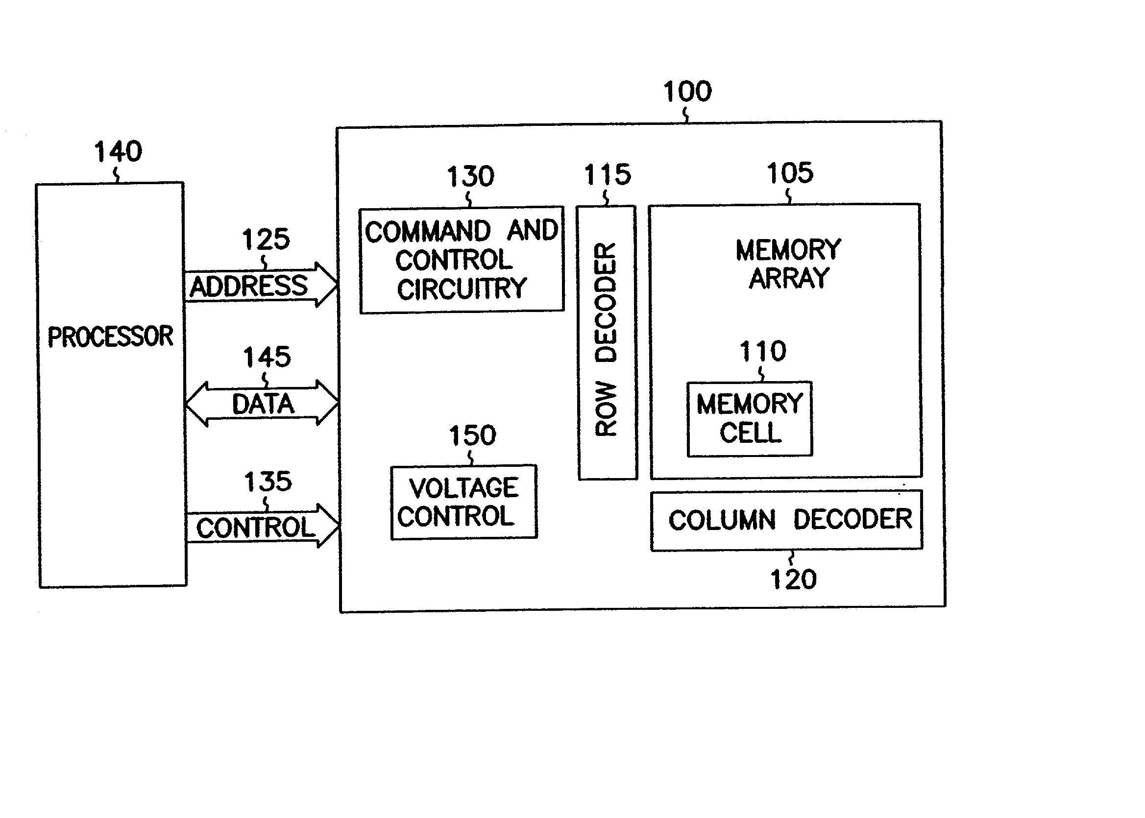
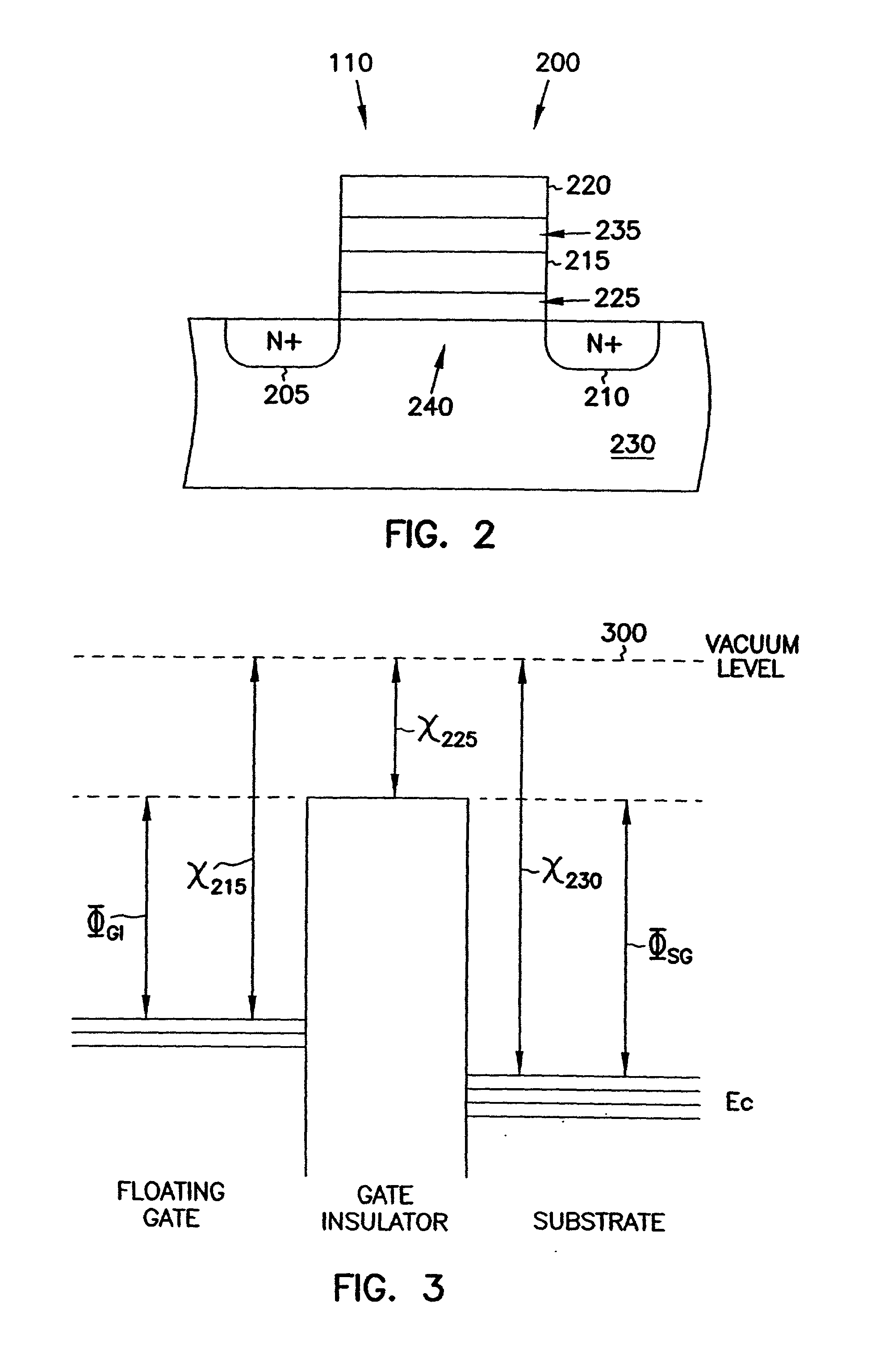
[0027] In the following detailed description of the invention, reference is made to the accompanying drawings which form a part hereof, and in which is shown, by way of illustration, specific embodiments in which the invention may be practiced. In the drawings, like numerals describe substantially similar components throughout the several views. These embodiments are described in sufficient detail to enable those skilled in the art to practice the invention. Other embodiments may be utilized and structural, logical, and electrical changes may be made without departing from the scope of the present invention. The teems wafer and substrate used in the following description include any semiconductor-based structure having an exposed surface with which to form the integrated circuit structure of the invention. Wafer and substrate are used interchangeably to refer to semiconductor structures during processing, and may include other layers that have been fabricated thereupon. Both wafer a...


PUM


Abstract

A floating gate transistor has a reduced barrier energy at an interface between a gallium nitride (GaN) or gallium aluminum nitride (GaAlN) floating gate an adjacent gate insulator, allowing faster charge transfer across the gate insulator at lower voltages. Data is stored as charge on the floating gate. The data charge retention time on the floating gate is reduced. The data stored on the floating gate is dynamically refreshed. The floating gate transistor provides a dense and planar dynamic electrically alterable and programmable read only memory (DEAPROM) cell adapted for uses such as for a dynamic random access memory (DRAM) or a dynamically refreshed flash EEPROM memory. The floating gate transistor provides a high gain memory cell and low voltage operation.

Description

CROSS REFERENCE TO RELATED APPLICATIONS[0001] This application is related to the following copending, commonly assigned U.S. patent applications: "DEAPROM HAVING AMORPHOUS SILICON CARBIDE GATE INSULATORS," serial number ______, "DYNAMIC ELECTRICALLY ALTERABLE PROGRAMMABLE READ ONLY MEMORY AND METHODS OF FABRICATION AND USE," serial number ______, "CARBURIZED SILICON GATE INSULATORS FOR INTEGRATED CIRCUIT," serial number ______, "SILICON CARBIDE GATE TRANSISTOR AND FABRICATION PROCESS," serial number ______,"TRANSISTOR WITH VARIABLE ELECTRON AFFINITY GATE AND METHODS OF FABRICATION AND USE," serial number ______, and "TRANSISTOR WITH SILICON OXYCARBIDE GATE AND METHODS OF FABRICATION AND USE," each of which is filed on even date herewith, and each of which disclosure is herein incorporated by reference.FIELD OF THE INVENTION[0002] The present invention relates generally to integrated circuit technology, including dynamic random access memories (DRAMs) and electrically erasable and pr...

Claims


Application Information

Patent Timeline
Patent Type & Authority Applications(United States)
IPC IPC(8): G11C16/04H01L29/423H01L29/43H01L29/788H10B12/00
CPCG11C16/0416H01L27/108H01L29/7885H01L29/432H01L29/7883H01L29/42324H10B12/00
Inventor FORBES, LEONARDAHN, KIE Y.
Owner MICRON TECH INC
Why Eureka
Try Eureka