Laser apparatus, laser annealing method, and manufacturing method of a semiconductor device

a manufacturing method and laser annealing technology, applied in the direction of individual semiconductor device testing, semiconductor/solid-state device testing/measurement, instruments, etc., can solve the problems of increasing production cost, increasing production cost, and many of these attachments

Inactive Publication Date: 2002-04-25
SEMICON ENERGY LAB CO LTD
View PDF44 Cites 140 Cited by
  • Summary
  • Abstract
  • Description
  • Claims
  • Application Information

AI Technical Summary

Benefits of technology

[0016] In particular, the second harmonic of the YAG laser has a frequency of 532 nm and is within a wavelength range (around 530 nm) in which reflection at an amorphous silicon film is the least when the amorphous silicon film is irradiated with the second YAG laser wave. In this wavelength range, in addition, the quantity of transmittable laser light through the amorphous semiconductor film is enough to efficiently irradiate again the amorphous semiconductor film from its back side using a reflective member. Moreover, the laser energy of the second harmonic is large, about 1.5 J / pulse at a maximum (in an existing pulse oscillation type YAG laser apparatus). When it is linearized, the length thereof in the longitudinal direction is therefore markedly lengthened to make it possible to irradiate a large area at once with laser light. These harmonics can be obtained by using a non-linear crystal.
[0018] Alternatively, the Q switch method (Q modulation switch method) that is often used in the YAG laser may be employed. This method is to sufficiently lower the Q value of a laser resonator in advance and to then rapidly raise the Q value, to thereby output sharp pulse laser having a very high energy value. The method is one of known techniques.
[0019] The solid state laser used in the present invention can output laser light as long as a solid crystal, a resonant mirror, and a light source for exciting the solid crystal are satisfied, basically. Therefore, maintenance thereof is not laborious unlike the excimer laser. In other words, the running cost of the solid state laser is significantly less as compared with the excimer laser, making it possible to greatly reduce the production cost of a semiconductor device. A decrease in number of the maintenance leads to an increase of the operating rate of the mass-production line, so that the throughput along the manufacturing steps is improved as a whole. This also contributes considerably to the reduction in production cost of the semiconductor device. Moreover, the solid state laser occupies a smaller area than the excimer laser does, which is advantageous in designing a production line.
[0020] In addition, to perform laser annealing by irradiating the front side and the back side of an amorphous semiconductor film with laser light allows obtainment of a crystalline semiconductor film with a larger crystal grain size than in prior art (where the amorphous semiconductor film is irradiated with laser light only from its front side). According to the applicant of the present invention, it is considered that irradiation of laser light onto the front side and the back side of an amorphous semiconductor film slows down the cycle of fusion and solidification of the semiconductor film, and that the crystal grain size is increased as a result.
[0021] The obtainment of a crystalline semiconductor film with a large crystal grain size leads to a considerable improvement of the performance of the semiconductor device. Taking a TFT as an example, enlargement of a crystal grain size allows reduction in number of crystal grain boundaries that may be contained in a channel formation region. That is, it allows fabricating a TFT that has one, preferably zero, crystal grain boundary in its channel formation region. Since the crystallinity of each crystal grain is such that it may substantially be regarded as a single crystal, to obtain a mobility (electric field effect mobility) equal to or higher than that of a transistor using a single crystal semiconductor is also possible.
[0022] Further, carriers cross the crystal grain boundaries extremely less frequently in the present invention to thereby reduce the fluctuation of ON current values (drain current when a TFT is in ON state), OFF current values (drain current when a TFT is in OFF state), threshold voltage, of S values, and electric-field effect mobility.

Problems solved by technology

However, Kr (krypton) gas and Xe (xenon) gas are very expensive, causing a problem of increase in production cost when recharge of the gas is frequent.
Many of these attachments are also expensive, taking part in increasing the production cost.
As seen in the above, a laser apparatus using excimer laser light does possess high ability but also possess drawbacks in that maintenance thereof is very troublesome and that the running cost (which means the costs required for operating the apparatus) is high for a laser apparatus for mass production.

Method used


Image

  • Laser apparatus, laser annealing method, and manufacturing method of a semiconductor device
  • Laser apparatus, laser annealing method, and manufacturing method of a semiconductor device
  • Laser apparatus, laser annealing method, and manufacturing method of a semiconductor device

Examples


embodiment 1

[0087] Embodiment 1

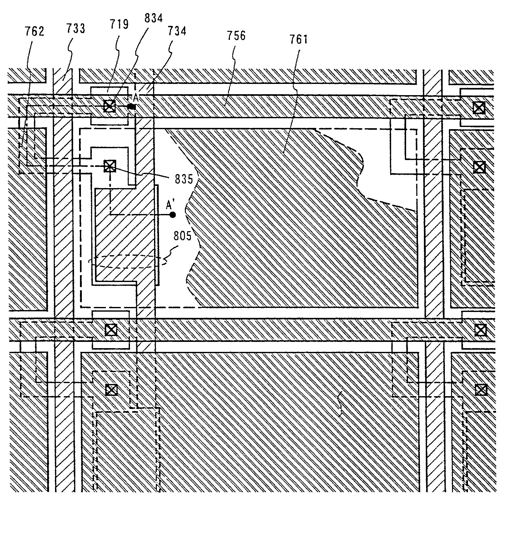
[0088] An embodiment of the present invention is described by using FIGS. 7A to 9C. A method for manufacturing a pixel TFT and a storage capacitor of the pixel section, and an n-channel TFT and a p-channel TFT of the driver circuit disposed in the periphery of the pixel section, at the same time, is described here.

[0089] In FIG. 7A, barium borosilicate glass or aluminoborosilicate glass as typified by Corning #7059 glass and #1737 glass can be used for a substrate 701. Besides these glass substrates, plastic substrates not having optical anisotropy such as polyethylene terephthalate (PET), polyethylene naphthalate (PEN), polyethersulfone (PES), etc. can also be used.

[0090] A base film 702 comprising such as a silicon oxide film, a silicon nitride film or a silicon oxynitride film is formed over the surface of the substrate 701, on which TFT is to be formed, in order to prevent the diffusion of impurities from the substrate 701. For example, a laminate of the silic...

embodiment 2

[0145] Embodiment 2

[0146] The example shown in Embodiment 1 is crystallization of an amorphous semiconductor film by using the methods described in Embodiment Modes 1 to 3 to perform laser annealing on the film. In the example, the laser annealing may be performed instead on a semiconductor film that has been crystallized to a certain degree but not thoroughly.

[0147] That is, the laser annealing in accordance with the present invention is also effective in the case where a crystalline semiconductor film that has been crystallized by furnace annealing is further projected to laser annealing to enhance its crystallinity.

[0148] To be specific, the laser annealing method of Embodiment Modes 1 to 3 may be used in the laser irradiation step described in Japanese Patent Application Laid-open No. Hei 7-321339, Japanese Patent Application Laid-open No. Hei 7-131034, and some other applications.

[0149] After the present invention is applied to the laser irradiation step of the above publicatio...

embodiment 3

[0150] Embodiment 3

[0151] This embodiment gives a description of a process of manufacturing an active matrix type liquid crystal display device using an active matrix substrate that is fabricated in accordance with Embodiments 1 and 2. First, as shown in FIG. 13A, spacers 901a to 901f are formed from a resin material by patterning on an active matrix substrate that is in a state illustrated in FIG. 9C. Alternatively, a known spherical silica or the like may be dispersed and used as the spacer.

[0152] In this embodiment, as the spacers 901a to 901f made of a resin material, NN 700 produced by JSR is applied by a spinner and is then formed into a given pattern through exposure and development treatment. Further, it is heated in a clean oven or the like at a temperature of 150 to 200.degree. C. to cure. The thus formed spacers may vary in shape depending on exposure conditions and development treatment conditions. A preferable shape for the spacers is a column with flat top, because it ...


PUM


Abstract

To provide a laser apparatus and a laser annealing method with which a crystalline semiconductor film with a larger crystal grain size is obtained and which are low in their running cost. A solid state laser easy to maintenance and high in durability is used as a laser, and laser light emitted therefrom is linearized to increase the throughput and to reduce the production cost as a whole. Further, both the front side and the back side of an amorphous semiconductor film is irradiated with such laser light to obtain the crystalline semiconductor film with a larger crystal grain size.

Description

[0001] 1. Field of the Invention[0002] The present invention relates to a method of annealing a semiconductor film with the use of laser light (hereinafter referred to as laser annealing) and to a laser apparatus for performing the laser annealing (an apparatus including a laser and an optical system for leading laser light output from the laser to a process object). The invention also relates to a semiconductor device fabricated by a manufacturing process that comprises the laser annealing step, and to the manufacturing process. The semiconductor device here includes an electro-optical device such as a liquid crystal display device and an EL display device, and an electronic device having the electro-optical device as one of its components.[0003] 2. Description of the Related Art[0004] An advance has been made in recent years in development of thin film transistors (hereinafter referred to as TFTs), and TFTs using polycrystalline silicon films (polysilicon films) as crystalline sem...

Claims


Application Information

Patent Timeline
IPC IPC(8): H01L21/20
CPCH01L21/2026Y10S438/904H01L27/1285H01L21/02691H01L21/02683H01L21/02532H01L21/02488H01L21/02422H01L21/02595
Inventor YAMAZAKI, SHUNPEIOHTANI, HISASHITANAKA, KOICHIROKASAHARA, KENJIKAWASAKI, RITSUKO
Owner SEMICON ENERGY LAB CO LTD
Why Eureka
Try Eureka