
Surface mounting type planar magnetic device and production method thereof

a planar magnetic and surface mounting technology, applied in the direction of recording information storage, instruments, transportation and packaging, etc., can solve the problems of obstructing the thinning of a power supply unit, the production cost of the planar inductors is sure to rise with respect to the conventional magnetic device, and the production cost of the planar inductors is sure to ris

Inactive Publication Date: 2001-09-27
KK TOSHIBA +1
View PDF0 Cites 47 Cited by
  • Summary
  • Abstract
  • Description
  • Claims
  • Application Information

AI Technical Summary

Benefits of technology

[0026] The thickness of the planar coil is 10 .mu.m or more to 100 .mu.m or less. To reduce loss by DC resistance of the coil, it is effective to enlarge a sectional area of the coil as well as reduce resistivity of coil material as described above. At this time, if the coil thickness is decreased, the coil width is increased. AC resistance R(f) of a N-turn coil under frequency f is expressed in the expression (2). 2 R ( f ) = Rdc [ 1 +4 2f 2tcd 412 2 ( Bk 2 lk ) lk ] ( 2 )
[0044] Bi.sub.2O.sub.3 has an effect of reducing the baking temperature like CuO. If it exceeds 10 mol %, inductance deteriorates although the baking temperature drops. Therefore, the upper limit is set to 10 mol %.
[0047] Next, the lower ferrite magnetic film formed on the substrate is baked together with the substrate at 900.degree. C. to 1250.degree. C., it is cooled down to room temperature. If Si is employed for the substrate, a warp occurs in the substrate / lower ferrite magnetic film composite material because the thermal expansion of the ferrite magnetic film is 9-10.times.10.sup.6 / K although the thermal expansion of the substrate is 2.4.times.10.sup.6 / K. As a result, a trouble may occur in post process such as planar coil production step. This problem can be solved by introducing cracks into the ferrite magnetic film positively so as to reduce an area surrounded by the cracks. In the ferrite magnetic film for the magnetic device formed on the substrate, preferably, a number of cracks are formed at least on the surface of ferrite magnetic film on an opposite side not in contact with the substrate and an average of diameters of circles converted from the areas surrounded by the cracks is less than 100 .mu.m. Meanwhile, if a crack is produced in the ferrite magnetic film, the crack reaches an edge of the film. If it is intended to just restore the warp, this can be also achieved by introducing several cracks. However, if the crack interval is large so that the area surrounded by the cracks is increased, leaking magnetic flux is generated, thereby producing new problems such as reduction of inductance by diamagnetic field and separation of the ferrite magnetic film. For the reason, the number of cracks is increased so as to reduce each area surrounded by the cracks. Consequently, distortion generated in the ferrite magnetic film is released so that the aforementioned problem never occurs. The area of a portion surrounded by the cracks is expressed by equivalent diameter. The equivalent diameter refers to the diameter of a circle converted from the area of a portion surrounded by the cracks. If the average of the equivalent diameter of each portion surrounded by the cracks exceeds 100 .mu.m, the aforementioned leaking magnetic flux occurs or the ferrite magnetic film becomes likely to be separated. Therefore, the upper limit is set to 100 .mu.m or less. Meanwhile, the depth of the crack may be only in the surface of the film or may reach the surface of the substrate. Although a method for generating such a crack is not restricted to any particular one, but the crack may be generated by reducing the baking temperature to a temperature lower than usually, for example, not more than 920.degree. C. or increasing the cooling velocity so as to be higher than 5.degree. C. per minute. Further, it is permissible to add additional material for reducing grain boundary strength, for example, V.sub.2O.sub.5, In.sub.2O.sub.3 into film so as to reduce mechanical strength of the film.

Problems solved by technology

However, these components are difficult to thin thereby obstructing thinning of a power supply unit.
However, these conventional planar inductors have problems in terms of production cost and characteristic.
That is, because metal magnetic film of 6 to 7 .mu.m is formed by spattering method and an insulating layer needs to be formed between the metal magnetic film and the planar coil, production cost for the planar inductor is sure to rise with respect to the conventional magnetic device.
Because the planar inductor is driven by high frequency in MHz band, power loss is increased by generation of eddy current inside metal magnetic film which is electrically conductive.
As for another characteristic problem, because upper and lower metal magnetic layers oppose each other through a slight nonmagnetic space, vertical alternate magnetic flux intersects the planar coil, so that eddy current is generated thereby increasing power loss.
However, it cannot be said that the characteristics have been improved sufficiently.
According to the conventional technology, because wire bonding method is employed to connect wires to a wired substrate, surface mount technology (SMT) cannot be applied, thereby leading to increase of production cost.
Although copper sulfate plating bath is employed for Cu, silver cyanide plating bath is employed for Ag, providing with a poor work efficiency.
Further, Ag needs higher cost than Cu and has a problem in migration.
Although the printing / baking method is often employed for chip inductor used for signal, this method has a problem that the resistivity is deteriorated because of mixture of binder component and incomplete baking.
In case of the inverse taper, there is generated a problem in adhesion because a contact area with the lower ferrite layer is small and upon production, upper ferrite paste is not fed around the planar coil well, so that a gap is generated between the coil and ferrite magnetic film, thereby producing problem on production such as increased disparity of inductance.
Therefore, it is evident that increase of the coil line width d is not preferable because it induces increase of coil loss due to vertical alternate magnetic field.
However, there occurs a new problem such as magnetic field ripple in magnetic film.
Although the baking temperature drops if CuO exceeds 20 mol %, inductance deteriorates.
However, the film thickness is increased so that defects such as separation of the ferrite magnetic film often occur.
As a result, a trouble may occur in post process such as planar coil production step.
Meanwhile, if a crack is produced in the ferrite magnetic film, the crack reaches an edge of the film.
However, if the crack interval is large so that the area surrounded by the cracks is increased, leaking magnetic flux is generated, thereby producing new problems such as reduction of inductance by diamagnetic field and separation of the ferrite magnetic film.
If a contact area with the external electrode is reduced too much, local heat is generated at the contact portion, thereby leading to such troubles as reduction of power efficiency at power supply and melt-down of the coil at worst.
If the surface of the coil terminal portion is contaminated in halfway process, conduction failure is likely to occur.
At this time, local heat is generated at a defective portion, thereby power efficiency at the power supply dropping or at worst a fatal trouble being generated such as destruction of the magnetic device.
On the other hand, if the baking temperature is less than 900.degree. C., the baking of the ferrite magnetic film is not accelerated sufficiently, so that a large inductance is not obtained and film strength is weakened.
In case of the inverse taper as shown in FIG. 16, area where the planar coil contacts the lower ferrite magnetic film 13 is small so that there is a problem in adhesion performance.
Further, upper ferrite magnetic paste is not distributed evenly over the planar coil, so that a gap 31 is generated between the coil and ferrite magnetic film, thereby increasing disparity of inductance.

Method used


Image

  • Surface mounting type planar magnetic device and production method thereof
  • Surface mounting type planar magnetic device and production method thereof
  • Surface mounting type planar magnetic device and production method thereof

Examples


example b

(Example B)

[0080] Al.sub.2O.sub.3 was used as a substrate and a magnetic device was produced in the same process as the example A. These examples 3 and 4 are shown in Table 1. The characteristic of the magnetic device under the condition of 5 MHz is shown in Table 1 as examples 3 and 4. This table indicates that any substrate indicates an excellent characteristic.

1 TABLE 1 Substrate Inductance (.mu.H) Quality factor Q Example 1 Si 2.0 12 Example 2 --2.1 13 Example 3 Al.sub.2O.sub.3 2.2 13 Example 4 -- 2.0 15

[0081] Quality factor Q is expressed by the expression (4).

Q=2.pi.f L / Rs (4)

[0082] where f=frequency (Hz), Rs (loss factor of inductance)=Rac +Rdc

[0083] Rac: AC resistance of inductance

[0084] Rdc: Dc resistance of inductance

[0085] The quality factor Q, was desired to exceed ten.

example c

(Example C)

[0086] Spiral arrangement, series arrangement of spiral, parallel arrangement of spiral and meander arrangement were used and a magnetic device shown in Table 2 was produced in the same process as the example A. Respective characteristics (under the condition of 5 MHz) are indicated in Table 2 as examples 5 to 8. The number of turns in the meander coil here refers to the number of folds. According to this Table 2, it is found that when the spiral coil is used, an inductance larger than the meander coil can be obtained and that two spiral coils are connected in series same as FIG. 13 and FIG. 14 such that mutual inductance between the coils is positive, an inductance twice or more larger than when a single spiral coil is used can be obtained.

2 TABLE 2 Number of Quality Coil Turns Inductance factor Specification N (.mu.H) Q Example 5 Meander 3 0.3 10 Example 6 Spiral 3 0.8 15 Example 7 Arrangement of 3 + 3 2.0 12 Spiral in Series same as FIG. 13 Example 8 Arrangement of 3 +...

example d

(Example D)

[0087] The condition of this example including the structure of coil is the same as the example A except that Cu, Ni and Ag shown in Table 3 are used as the coil material. In each case, an inductance and direct resistance Rdc, under the condition of 5 MHz was measured. By loading the coil on a DC / DC converter shown in FIG. 17 as a chalk coil and driving it at rectangular wave of 0.5 in pulse interval ratio (duty ratio) and 5 MHz, power efficiency was obtained. The power efficiency was obtained by a ratio of output power relative to input power in a circuit shown in FIG. 17. In the DC / DC converter 40 shown in FIG. 17, a pulse from a pulse generator 45 is applied to a circuit comprising a capacitor 42, a chalk 43 and a MOS-FET 44 so as to convert DC input 41 to alternate current and then the voltage is raised. Then, DC output 48 is outputted to a rectifying circuit comprising a diode 46 and a capacitor 47. Table 3 shows measurement results as the examples 9 to 11. It is fou...


PUM

PropertyMeasurementUnit
thicknessaaaaaaaaaa
thicknessaaaaaaaaaa
diametersaaaaaaaaaa

Abstract

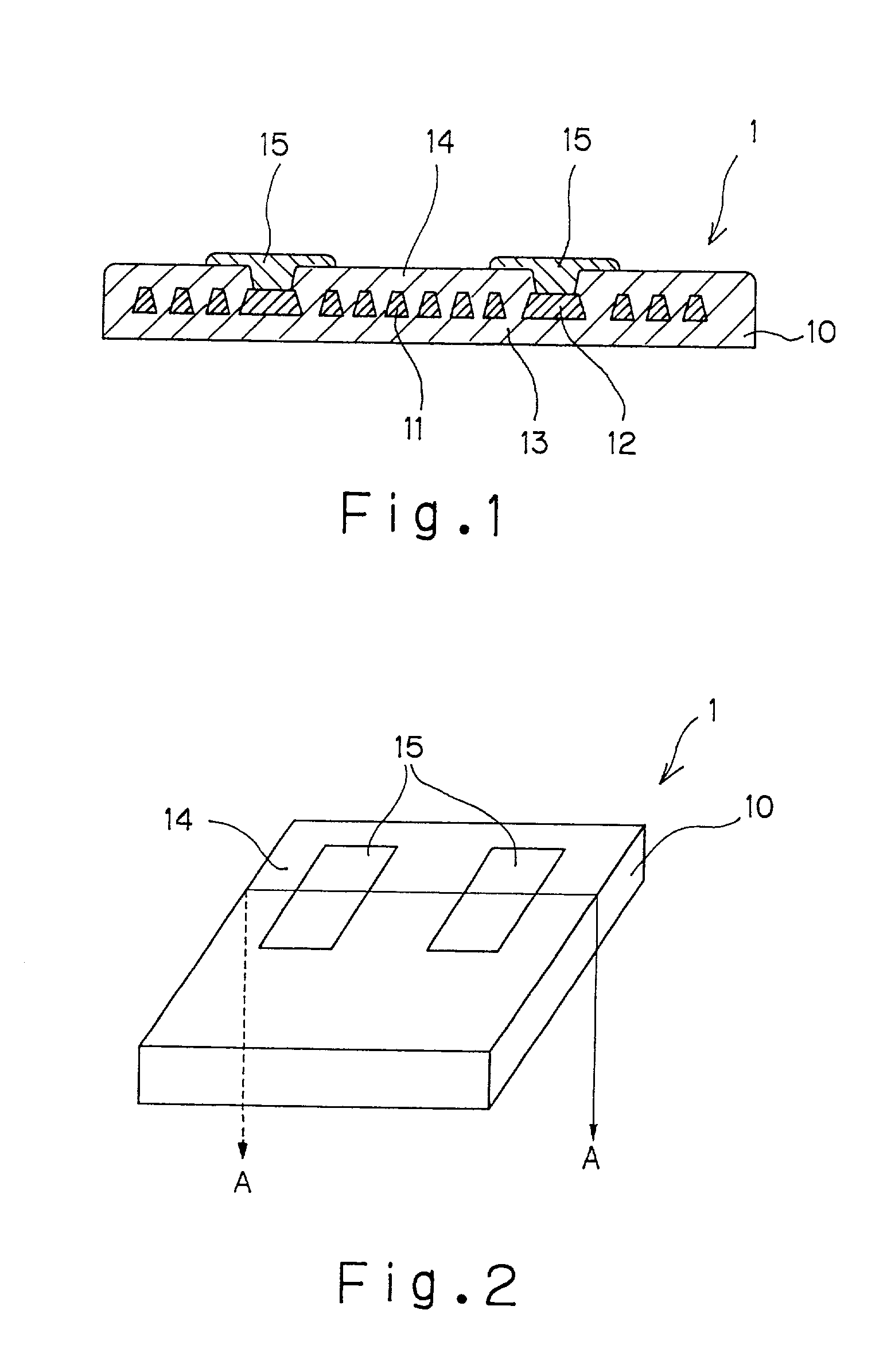
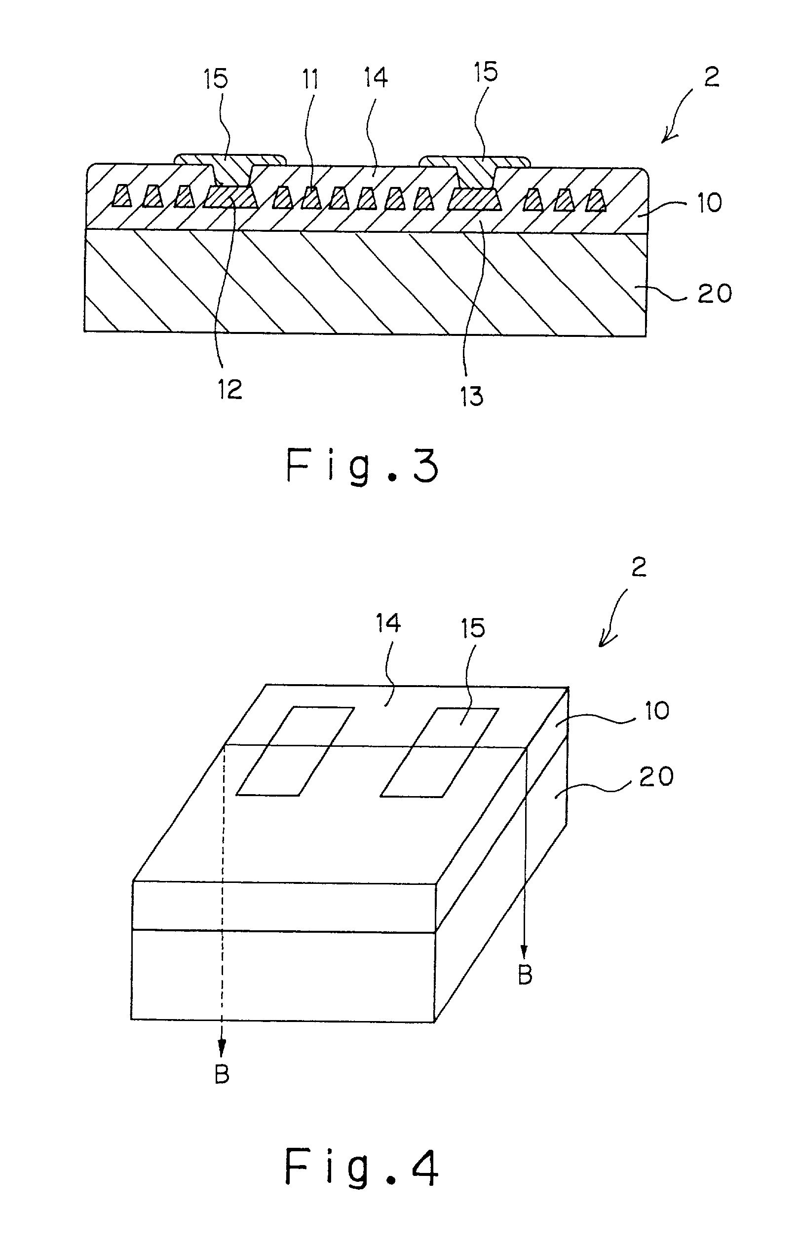
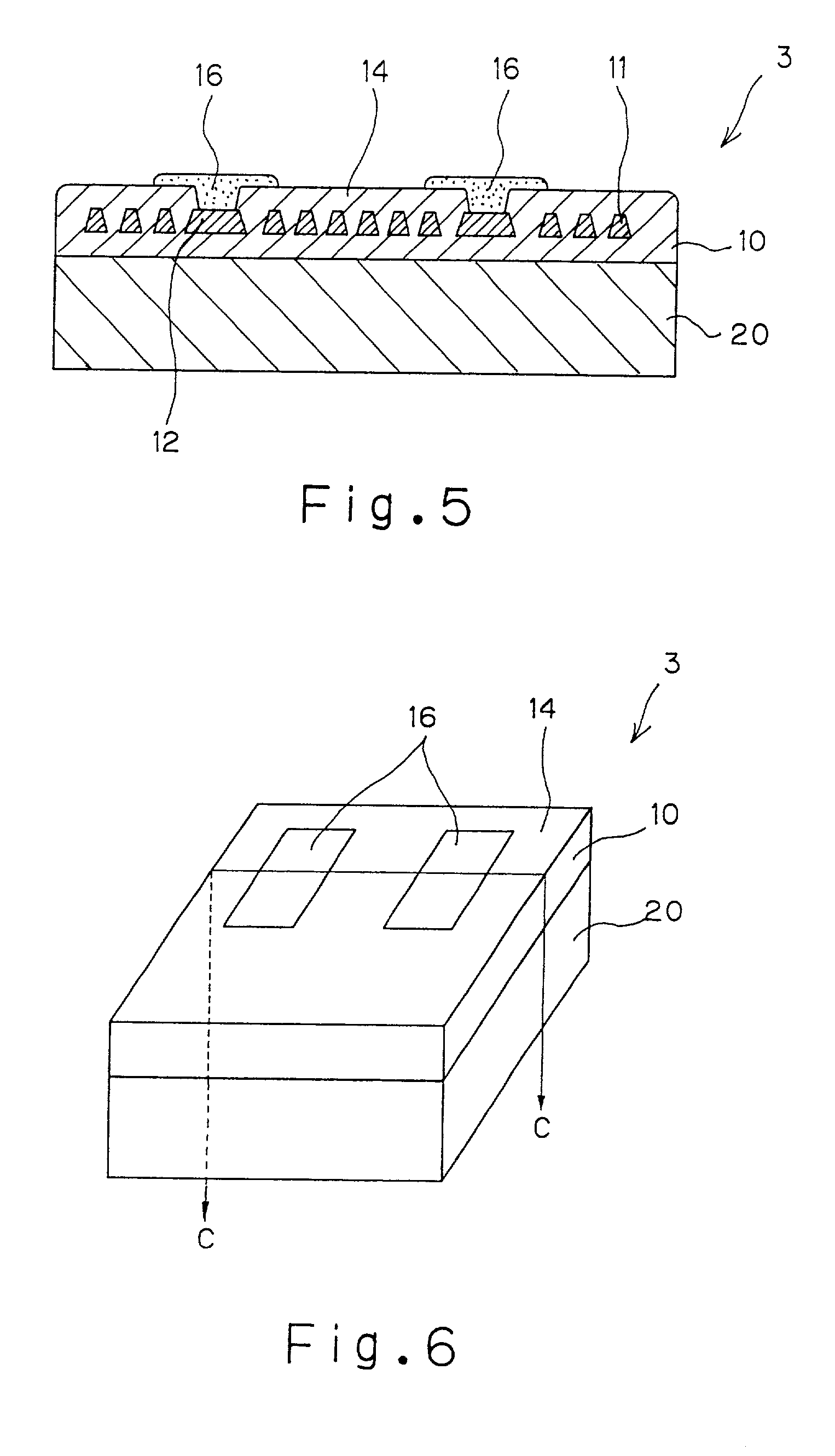
This invention provides a surface mounting type planar magnetic device comprised of upper ferrite magnetic film, lower ferrite magnetic film and a planar coil interposed therebetween. For applying surface mount technology, an opening is formed in the upper ferrite magnetic film above a coil terminal portion and then, an external electrode conductive with the coil terminal portion through the opening is formed on the upper ferrite magnetic film. Further, this surface mounting type planar magnetic device is of a thin structure and can be mounted on the surface of a printed board. Its power loss is small, its inductance is large, its frequency characteristic is excellent, the disparity of the characteristic is small and its reliability is excellent.

Description

[0001] 1. Field of the Invention[0002] The present invention relates to a surface mounting type planar magnetic device and production method thereof.[0003] 2. Description of the Related Art[0004] In recent years, use of portable apparatuses driven by battery such as mobile phone and notebook-type personal computer has been accelerated. Since before, reduction of the weight and size of such portable apparatuses has been demanded and in addition to this demand, recently, higher functions such as communication function, display function and high-speed processing function for a large amount of information including image data have been also requested. Correspondingly, a demand for a power supply capable of transforming a single voltage from a battery to voltage levels necessary for various mounted devices such as CPU, LCD module, and communication power amplifier has been increased. Thus, to achieve the higher function as well as reduction of the size and weight, it has been an importan...

Claims


Application Information

Patent Timeline
Patent Type & Authority Applications(United States)
IPC IPC(8): H01F10/20H01F27/28H01F17/00H01F17/04H01F27/29H01F37/00
CPCH01F17/0006H01F17/04H01F27/292Y10T428/32Y10T428/12431
Inventor MIZOGUCHI, TETSUHIKOINOUE, TETSUOYATABE, SHIGERUFUKUDA, YASUTAKATACHI, YOSHIHITO
Owner KK TOSHIBA
Learn More