Suface procesing method by blowing submicron particles
a technology of submicron particles and suface, which is applied in the direction of metal rolling stands, metal-working apparatus, metallic material coating processes, etc., can solve the problems of troublesome maintenance of the apparatus, low processing rate of the etching method, and needing an expensive apparatus, so as to enhance the stirring effect of the compressed air and maintain the stirring effect effectively
- Summary
- Abstract
- Description
- Claims
- Application Information
AI Technical Summary
Benefits of technology
Problems solved by technology
Method used
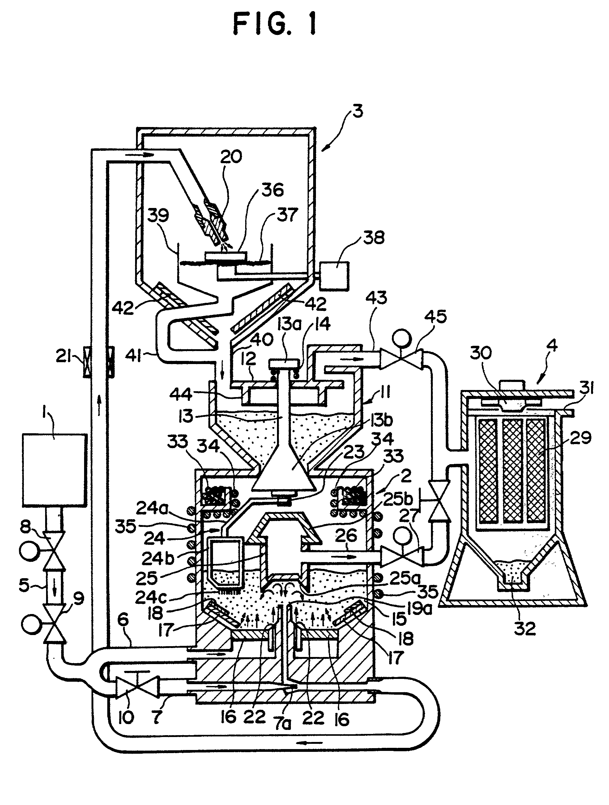
Image

Examples
example 2
[0095] Alumina submicron particles of an average particle size of 0.6 .mu.m were blown against the surface of a ferrite substrate under the same surface processing conditions as those employed for Example 1. A dense alumina thin film was formed.
[0096] A dense alumina thin film was formed also by using alumina submicron particles of an average particle size of 0.2 .mu.m.
comparable example 1
[0097] Alumina submicron particles of an average particle size of 5 .mu.m were blown against the surface of a ferrite substrate under the same surface processing conditions as employed in Example 1. The alumina submicron particles were not deposited at all and the surface of the ferrite substrate was etched.
example 3
[0098] Alumina submicron particles of an average particle size of 0.6 .mu.m were blown against the surface of a ferrite substrate for etching.
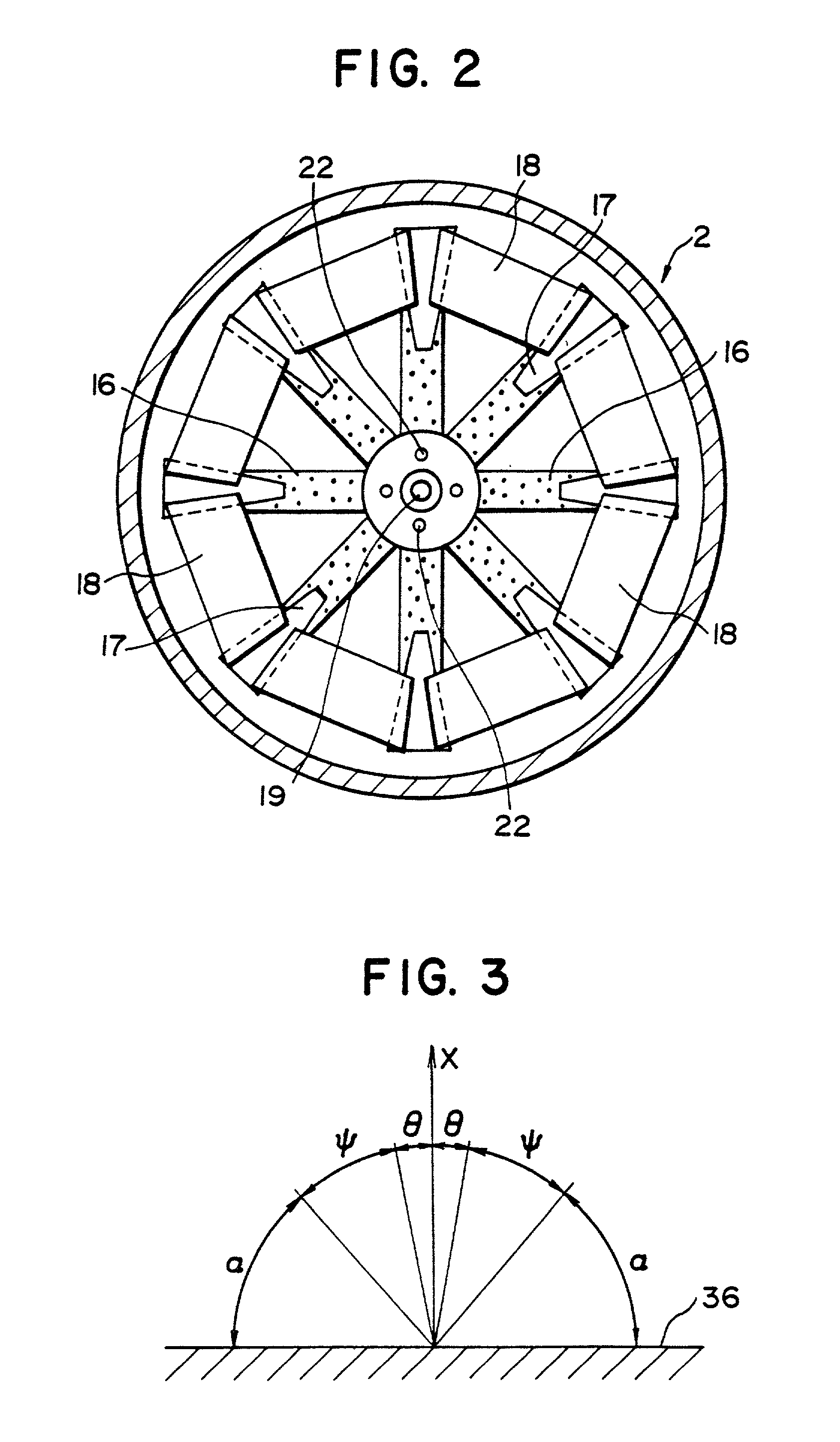
[0099] Surface processing conditions were the same as those employed in Example 1, except that the incident angle was 40.degree. C.
[0100] The width of lines forming a pattern to be formed by etching was 50 .mu.m. A Photosensitive urethane rubber film of 5 .mu.m in thickness was used as an etching resist.
[0101] During the etching process, the ferrite substrate was rotated at 30 rpm. The alumina submicron particles were blown for sixty seconds.
[0102] The surface of the ferrite substrate was etched by a depth of 2 .mu.m, the inclination of the side surfaces of the lines of the pattern was about 60.degree., and the etched portions were mirror-finished in a surface roughness R.sub.max of 0.06 .mu.m.
PUM
| Property | Measurement | Unit |
|---|---|---|
| Angle | aaaaa | aaaaa |
| Angle | aaaaa | aaaaa |
| Angle | aaaaa | aaaaa |
Abstract
Description
Claims
Application Information
 - R&D
- Intellectual Property
- Life Sciences
- Materials
- Tech Scout
- Unparalleled Data Quality
- Higher Quality Content
- 60% Fewer Hallucinations
Browse by: Latest US Patents, China's latest patents, Technical Efficacy Thesaurus, Application Domain, Technology Topic, Popular Technical Reports.
© 2025 PatSnap. All rights reserved.Legal|Privacy policy|Modern Slavery Act Transparency Statement|Sitemap|About US| Contact US: help@patsnap.com