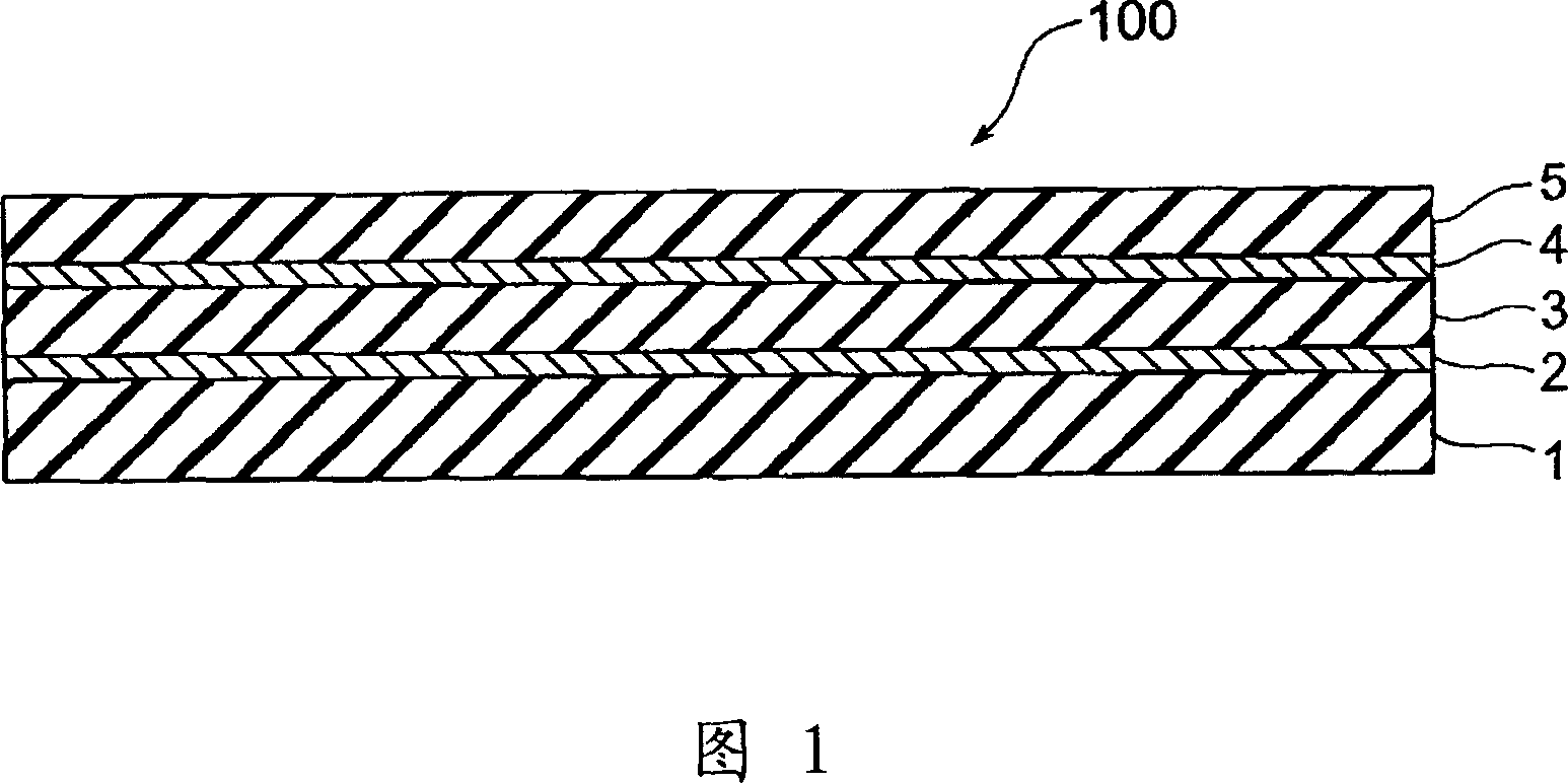
Circuit substrate and manufacturing method thereof
A technology of circuit substrate and manufacturing method, which is applied in the fields of printed circuit manufacturing, circuit substrate material, multilayer circuit manufacturing, etc. It can solve the difficulty of transmitting signals, the difficulty of providing high-quality signal current in high-frequency areas, and the difficulty of circuit substrates adapting to high-frequency signals, etc. problem, to achieve low adhesion, suppress crosstalk or radiation noise
- Summary
- Abstract
- Description
- Claims
- Application Information
AI Technical Summary
Problems solved by technology
Method used
Image
Examples
Embodiment 1
[0126] 8-Ethyl-tetracyclo[4.4.0.1 2,5 .1. 7,10 ] Ring-opening polymerization of dodec-3-ene followed by hydrogenation reaction to obtain a hydrogenated polymer with number average molecular weight (Mn)=31,200, weight average molecular weight (Mw)=55,800, Tg=about 140°C. The hydrogenation rate of the obtained hydrogenated polymer is above 99%.
[0127] 100 parts of this hydrogenated polymer, 40 parts of maleic anhydride and 5 parts of dicumyl peroxide were dissolved in 250 parts of tert-butylbenzene, and the reaction was carried out at 140° C. for 6 hours. The obtained reaction product solution was added to 1000 parts of isopropanol to solidify the reaction product, and the obtained solid was vacuum-dried at 100° C. for 20 hours to obtain a maleic acid-modified hydrogenated polymer. This maleic acid-modified hydrogenated polymer had Mn=33,200, Mw=68,300, Tg was 170° C., and the maleic anhydride group content was 25 mol%.
[0128] Make 100 parts of maleic acid modified hydrog...
Embodiment 2
[0140] Except that the surface of the first electrical insulating layer 3 of the above-mentioned Example 1 was immersed in a permanganate treatment bath for 30 minutes, a multilayer circuit board B with wiring patterns on both sides and 4 layers was obtained in the same manner as in Example 1. The surface roughnesses of the first conductor layer 2 and the first electrical insulating layer 3 measured in the process of producing the substrate were 70 nm and 350 nm, respectively. The evaluation results are shown in Table 1 below.
Embodiment 3
[0142] Make 100 parts of the aforementioned maleic acid modified hydrogenated polymer, 40 parts of bisphenol A bis(propylene glycol glycidyl ether) ether, 0.1 part of 1-benzyl-2-phenylimidazole (curing accelerator), 5 parts of 2- [2-Hydroxy-3,5-bis(a,a-dimethylbenzyl)phenyl]benzotriazole (laser processability enhancer), 1 part of tris(3,5-di-tert-butyl-4 -Hydroxybenzyl)-isocyanurate, 10 parts of liquid polybutadiene (B-1000, manufactured by Nippon Petrochemical Co., Ltd.), 156 parts of ferrite material ( Toda Kogyo Co., Ltd.) was dissolved in a mixed organic solvent composed of 222 parts of xylene and 555 parts of cyclopentanone, uniformly dispersed and mixed using a planetary mixer, and a varnish containing fine magnetic powder was obtained.
[0143] A multilayer circuit board C with wiring patterns having 4 layers on both sides was produced in the same manner as in Example 1 except that the varnish containing fine magnetic powder was used. The surface roughnesses Ra of the ...
PUM
 Abstract
Description
Claims
Application Information
 - Generate Ideas
- Intellectual Property
- Life Sciences
- Materials
- Tech Scout
- Unparalleled Data Quality
- Higher Quality Content
- 60% Fewer Hallucinations
Browse by: Latest US Patents, China's latest patents, Technical Efficacy Thesaurus, Application Domain, Technology Topic, Popular Technical Reports.
© 2025 PatSnap. All rights reserved.Legal|Privacy policy|Modern Slavery Act Transparency Statement|Sitemap|About US| Contact US: help@patsnap.com


