Tech. for etching capable of controlling grid structural length
A technology of structure length and gate control, applied in semiconductor/solid-state device manufacturing, electrical components, semiconductor devices, etc., can solve the problems of smaller key dimensions, secondary initial leakage of MOS transistors, and achieve the effect of maintaining integrity
- Summary
- Abstract
- Description
- Claims
- Application Information
AI Technical Summary
Problems solved by technology
Method used
Image
Examples
Embodiment Construction
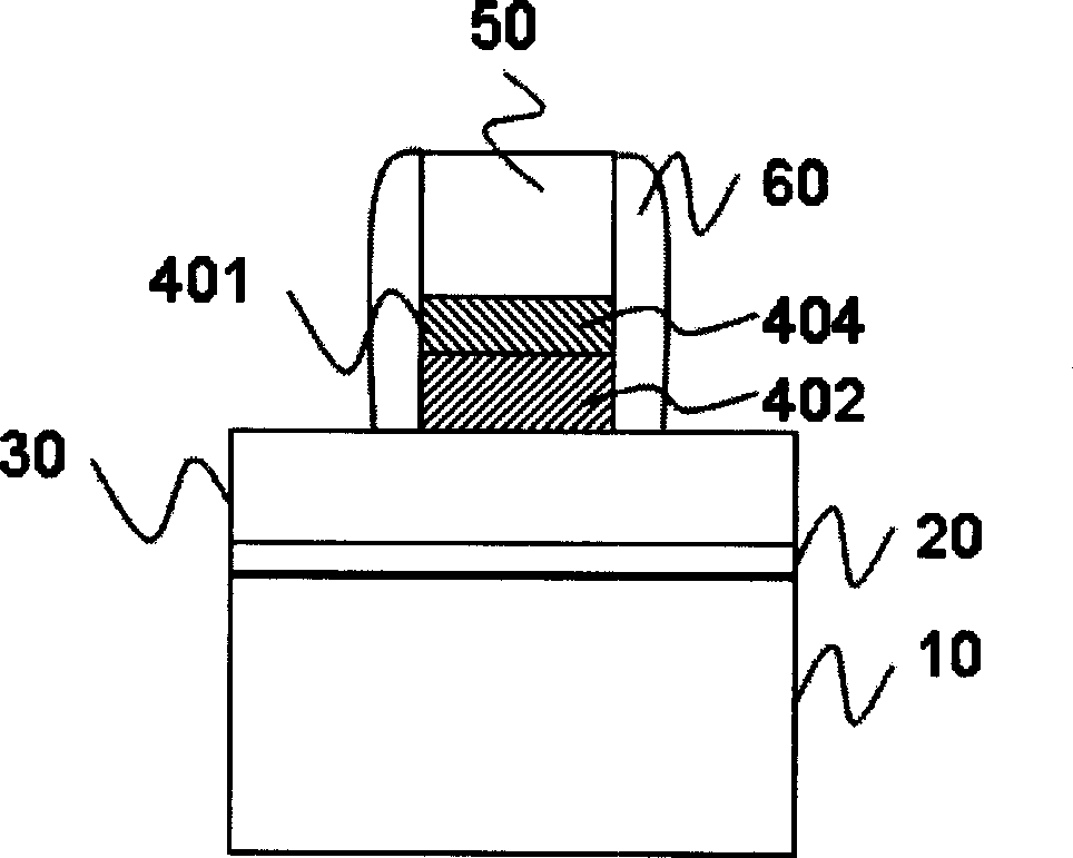
[0023] Figure 1 to Figure 4 It is a cross-sectional view of each step of making the gate structure of the present invention; Figure 5 It is a schematic flow chart of the etching process that can control the length of the gate structure in the present invention. In order to describe this preferred embodiment in more detail, please refer to figure 1 and Figure 5 .
[0024] First, proceed to step S10, providing such as figure 1 A silicon substrate 10 is shown, and a gate oxide layer 20 , a polysilicon layer 30 , a hard mask layer 40 and a patterned photoresist 50 are sequentially deposited on the silicon substrate 10 by using chemical vapor deposition technology. The hard mask layer 40 is composed of a TEOS layer 402 and a dielectric layer 404. The TEOS layer 402 is located under the dielectric layer 404. The entire hard mask layer 40 is set because the hard mask layer 40 is patterned The photoresist 50 can also provide a better etching selectivity ratio. When the polysi...
PUM
 Abstract
Description
Claims
Application Information
 - R&D
- Intellectual Property
- Life Sciences
- Materials
- Tech Scout
- Unparalleled Data Quality
- Higher Quality Content
- 60% Fewer Hallucinations
Browse by: Latest US Patents, China's latest patents, Technical Efficacy Thesaurus, Application Domain, Technology Topic, Popular Technical Reports.
© 2025 PatSnap. All rights reserved.Legal|Privacy policy|Modern Slavery Act Transparency Statement|Sitemap|About US| Contact US: help@patsnap.com


