Method for fabricating a mosfet and reducing line width of gate structure

A technology of oxide semiconductors and manufacturing methods, which is applied in semiconductor/solid-state device manufacturing, transistors, semiconductor devices, etc., and can solve problems such as reduced process margins, difficulty in forming correct line widths, and inability to form metal silicide layers well , to achieve the effect of easy control, lower thermal budget and wide process margin

Inactive Publication Date: 2007-04-25
MACRONIX INT CO LTD
View PDF4 Cites 0 Cited by
  • Summary
  • Abstract
  • Description
  • Claims
  • Application Information

AI Technical Summary

Problems solved by technology

[0004] Due to the narrowing of the gate line width, it will be difficult to form the correct line width in the lithography process of defining the gate line width, which means that the difficulty of the lithography process of defining the gate line width will increase, and will lead to other Process Margin Reduction
[0005] Moreover, when the line width of the gate is reduced below a certain size, a so-called line width effect (line width effect) will occur for the forming step of the metal silicide layer, that is, the metal silicide layer will not be well formed. Formed on gate structures with smaller line widths
[0006] Also, as the components shrink, so does the profile of the source / drain extension, however, since the metal silicide layer is formed after the source / drain extension, the source / drain The pole extension must bear the thermal budget of the tempering process of the metal silicide layer, making the profile of the source / drain extension less controllable

Method used


Image

  • Method for fabricating a mosfet and reducing line width of gate structure
  • Method for fabricating a mosfet and reducing line width of gate structure
  • Method for fabricating a mosfet and reducing line width of gate structure

Examples


Embodiment Construction

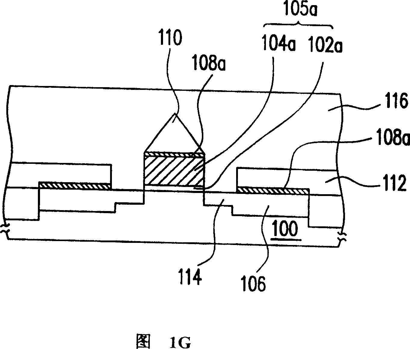
[0028] 1A to 1G are schematic cross-sectional flow diagrams illustrating a method for manufacturing a metal oxide semiconductor transistor according to a preferred embodiment of the present invention.

[0029] First, referring to FIG. 1A , a substrate 100 on which a gate structure 105 has been formed is provided, wherein the gate structure 105 is formed by sequentially stacking a gate dielectric layer 102 and a conductor layer 104. The material of the substrate 100 is, for example, The material of the silicon substrate and the gate dielectric layer 102 is, for example, silicon oxide; (not shown), and then pattern the dielectric material layer and the conductive material layer to form.

[0030] Next, referring to FIG. 1B , source / drain regions 106 are formed in the substrate 100 on both sides of the gate structure 105 by, for example, using the gate structure 105 as a mask to perform an ion implantation process on the substrate 100. , to form source / drain regions 106 in the su...


PUM


Abstract

A method for fabricating a MOSFET is provided. The method comprises: providing a substrate, the substrate having a gate structure; forming a drain region and a source region in the substrate, the drain region and the source region being on two sides of the gate structure respectively; forming a metal suicide layer on the surface of the gate structure, the drain region, and the source region; forming a patterned block on the metal silicide layer above the gate structure, and forming a first dielectric layer above the substrate except the gate strcutre, the patterned block being formed above the center of the gate structure and the metal silicide layer above the gate structure beside two sides of the patterned block being exposed; removing a portion of the metal silicide layer and a portion of the gate structure by using the patterned block as a mask; and forming a drain extension region and a source extension region in the substrate, beside two sides of the remaining gate structure.

Description

technical field [0001] The present invention relates to a method of manufacturing a semiconductor component, and in particular to a method of manufacturing a metal oxide semiconductor transistor. Background technique [0002] With the increasing integration of integrated circuits, the area of ​​semiconductor components is gradually shrinking. Metal-oxide-semiconductor transistors have many advantages such as very small power consumption and are suitable for high-density integrated manufacturing. The most important and widely used basic electronic component in the manufacturing process. And in today's metal-oxide-semiconductor transistors, in order to overcome problems such as increased contact resistance between the gate and the wire, increased resistance-capacitance delay (RC Delay), and reduced operating speed of the component due to the narrowing of the gate line width, it is generally The countermeasure taken by Yan is to form a metal silicide on the gate in order to re...

Claims


Application Information

Patent Timeline
Patent Type & Authority Patents(China)
IPC IPC(8): H01L21/336H01L21/28H01L29/786H01L29/78
CPCH01L29/7833H01L29/665H01L21/28052H01L29/6659
Inventor 赖二琨
Owner MACRONIX INT CO LTD
Why Eureka
Try Eureka