Single electron memory having carbon nano tube structure and process for making it

A carbon nanotube and memory technology, applied in the field of single-electron memory, can solve problems such as limited integration, low device integration, and affecting device stability, and achieve the effects of reducing preparation steps and avoiding doping processes

Inactive Publication Date: 2006-06-28
INST OF PHYSICS - CHINESE ACAD OF SCI
View PDF0 Cites 1 Cited by
  • Summary
  • Abstract
  • Description
  • Claims
  • Application Information

AI Technical Summary

Problems solved by technology

However, maintaining the trend of continuous scale reduction is facing an extremely serious challenge, that is, the capacitance in the storage unit cannot be too small. If the capacitance is too small to provide enough electrons to the amplifier, the entire memory will be flooded by noise, and the The reliability of information storage cannot be guaranteed; at the same time, the number of electrons in each storage unit will become smaller and smaller with the further improvement of the integration of storage devices, and the MOS field effect transistors in the memory will gradually become unstable.
[0003] In order to continue to maintain the high-speed development of memory devices, people hope to replace traditional memory ...

Method used


Image

  • Single electron memory having carbon nano tube structure and process for making it
  • Single electron memory having carbon nano tube structure and process for making it
  • Single electron memory having carbon nano tube structure and process for making it

Examples


Embodiment 1

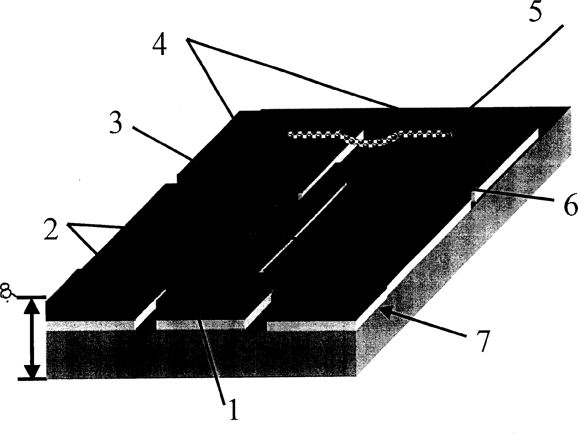
[0047] according to figure 1 A single-electron memory having a carbon nanotube structure of the present invention was fabricated.

[0048] Select silicon on insulator (SOI) material as the substrate, and use dry oxygen oxidation technology to oxidize and thin the single crystal silicon layer. The parameters are as follows: material crystal orientation , P type, resistivity 3Ωcm; silicon layer thickness is 40 nm, and the silicon dioxide layer is 50 nm thick. The single crystal silicon layer is heavily doped with arsenic to become an n-type semiconductor layer with a doping concentration of 6×10 13-2 .

[0049] The nanowire structure and the carbon nanotube crystal structure are prepared in the silicon layer on the insulator by electron beam lithography method and dry etching technology. The length of the nanowire 3 is 100 nanometers, the width is 30 nanometers, and the height is 90 nanometers; the control gate 2 of each nanowire is 60 nanometers wide, 60 nanometers long, and...

Embodiment 2

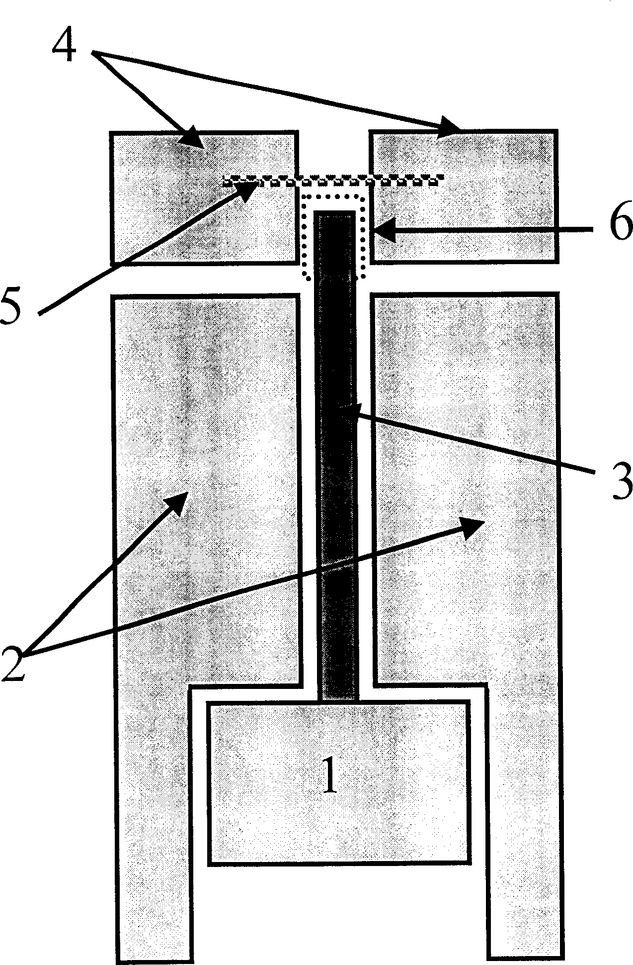
[0056] according to Figure 8 A single-electron memory having a carbon nanotube structure of the present invention was fabricated.

[0057]The preparation method of the nanowires is the same as that in Example 1, and the single-walled carbon nanotubes 5 are prepared and positioned using the in-situ growth technology of carbon nanotubes. Utilize the probe technology of atomic force microscope to place catalyst zone 9 on the inner side of gold electrode 4, grow carbon nanotube 5 in situ, and make the two ends of carbon nanotube have good electric contact with the electrode of carbon nanotube transistor; If growing Good contact is not achieved in the process, and the focused ion beam FIB technology can be used to achieve good contact between the carbon nanotube 5 and the electrode 4 of the carbon nanotube transistor. Finally, the device is packaged and wired.

Embodiment 3

[0059] On the single-electron memory device prepared in Example 1 or 2, carbon nanotubes are used as leads on each electrode.


PUM

PropertyMeasurementUnit
Lengthaaaaaaaaaa
Heightaaaaaaaaaa
Resistivityaaaaaaaaaa

Abstract

The invention discloses a single electron dynamic random access memory (DRAM) device and process for making it. The device uses the Si SOI material on the insulation layer as substrate, a nano line is made by etching processing in the Si layer of SOI, one end of the nano line is data cable pin, and there are two control grids parallel to the two sides of the namo lines at each side of them. the device also includes a carbon nano tube transistor. The memory unit is the part of the namo line which is longer the the control grid and extending into between the two electrode regions of the carbon nano transistor. By controlling several dozens or several electrons, the normal operation of the memory can be realized and without the influence of the random background charges, thus solving the problems such as stability, power consumption, radiation and grid leakage current faced in the development of the traditional memories, the invention also realizes the super-high density information storage under the low power consumption condition.

Description

technical field [0001] The invention relates to a memory device, in particular to a single-electronic memory designed and prepared by using carbon nanotubes. Background technique [0002] Memory accounts for 40% of the world's semiconductor market. Semiconductor products other than memory are updated every 2 years, while memory is a generation every 18 months. Taking the development of dynamic memory (DRAM) as an example, in 1988 Japan The line width of the lines on the silicon chip reached 0.8 microns, and the 4Mb DRAM came out, thus entering the era of ultra-large-scale integration ULSI; in 1992, the 16Mb chip with a line width of 0.5 microns was put into production; in 1994, the 64Mb chip with a line width of 0.35 microns was launched. Chip production; 0.13-micron 4Gb DRAM will soon be realized. However, maintaining the trend of continuous scale reduction is facing an extremely serious challenge, that is, the capacitance in the storage unit cannot be too small. If the ca...

Claims


Application Information

Patent Timeline
IPC IPC(8): H01L27/00H01L21/70B82B1/00B82B3/00G11C13/02
CPCG11C13/025B82Y10/00B82Y30/00G11C13/0033G11C2216/08
Inventor 孙劲鹏王太宏
Owner INST OF PHYSICS - CHINESE ACAD OF SCI
Why Eureka
Try Eureka