


Quick Research
Generate reliable direction feasibility study reports for your R&D in just a few steps.

Technical Q&A
Discover and master advanced knowledge NOW. Basics, ideas, possibilities, all at once.

Find Solutions
As an expert in R&D theories, this can generate solutions to your technical problems instantly.

Evaluate Feasibility
Analyze your overall solution with one click, know your potential R&D risks in advance.

Monitor Landscape
Get weekly tech updates, stay abreast of the latest tech innovations and key insights.
Groove silicon carbide MOSFET integrated with high-speed fly-wheel diode and preparation method
A freewheeling diode, silicon carbide technology, applied in semiconductor/solid-state device manufacturing, semiconductor devices, electrical components, etc., can solve the problems of high conduction voltage drop of SiC body diode, high density of JFET area, and increased dynamic loss of devices, etc. Achieve the effect of improving long-term reliability, reducing on-voltage and reducing Miller capacitance
- Summary
- Abstract
- Description
- Claims
- Application Information
AI Technical Summary
Problems solved by technology
Method used
Image

Examples
Embodiment 1
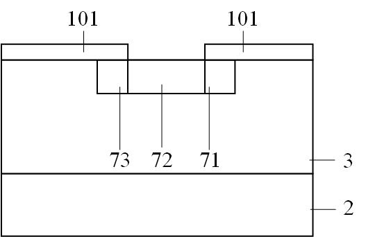
[0042] like figure 1 As shown, this embodiment provides a trench silicon carbide MOSFET with integrated high-speed freewheeling diode, including a backside ohmic contact alloy 1, an N-type doped silicon carbide substrate 2, an N-type doped silicon carbide epitaxial layer 3, a first P-type doped buried layer 41, second P-type doped buried layer 42, third P-type doped buried layer 43, first gate oxide layer 51, second gate oxide layer 52, first polysilicon 61, Two polysilicon 62, a first P-type doped well region 71, a second P-type doped well region 72, a third P-type doped well region 73, a first N-type doped source region 81, a second N-type doped well region 81 Doping source region 82, P-type doping source region 9, interlayer dielectric 10, front ohmic contact alloy 11;
[0043] On the plane formed by the x-axis and the y-axis, the N-type doped silicon carbide substrate 2 is located above the backside ohmic contact alloy 1; the N-type doped silicon carbide epitaxial layer 3...
Embodiment 2
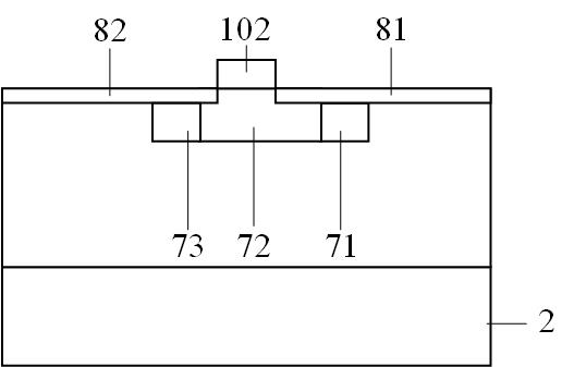
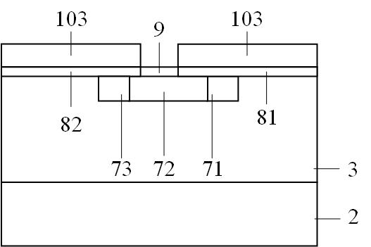
[0050] like Figure 2 to Figure 9 As shown, this embodiment provides a method for fabricating a trench silicon carbide MOSFET integrated with a high-speed freewheeling diode, including the following steps:
[0051] Step 1: An oxide layer is deposited on the N-type silicon carbide epitaxial wafer. After photolithography, an ion-implanted P-well ion-implantation mask layer 101 is formed, and then Al ion implantation is performed at a temperature of 300K~1000K to form a second P-type dopant. In the miscellaneous well region 72, at the same time, since the Al ion implantation in silicon carbide will cause lateral scattering, P-type doping scattering regions with laterally graded concentration will be simultaneously formed on the left and right sides of the second P-type doping well region 72, respectively. For the first P-type doped well region 71 and the third P-type doped well region 73, the following figure 2 structure. After the injection is completed, the mask layer is rem...
PUM
 Abstract
Description
Claims
Application Information
 - R&D Engineer
- R&D Manager
- IP Professional
- Industry Leading Data Capabilities
- Powerful AI technology
- Patent DNA Extraction
Browse by: Latest US Patents, China's latest patents, Technical Efficacy Thesaurus, Application Domain, Technology Topic, Popular Technical Reports.
© 2024 PatSnap. All rights reserved.Legal|Privacy policy|Modern Slavery Act Transparency Statement|Sitemap|About US| Contact US: help@patsnap.com