Memristor unit based on dual-ion regulation and preparation method thereof
A memristor and dual-ion technology, which is applied to the field of memristor units based on dual-ion regulation and their preparation, can solve problems such as inability to simulate complex synaptic functions more vividly, and achieve the effect of simple process
- Summary
- Abstract
- Description
- Claims
- Application Information
AI Technical Summary
Problems solved by technology
Method used
Image
Examples
specific Embodiment 1
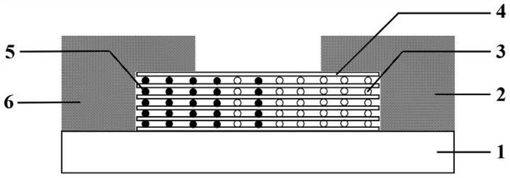
[0031] For specific reference figure 1 , the present invention provides a memristor unit based on dual ion regulation, comprising a substrate 1 and a first electrode 6 and a second electrode 2 arranged on the substrate 1 at intervals, the first electrode 6 and the second electrode 2 A dielectric layer 4 is inserted between 2. The dielectric layer 4 in this specific embodiment is a layered inorganic two-dimensional material. The dielectric layer 4 has a plurality of inter-units, and the van der Waals force is used between each unit. connection, the dielectric layer 4 has a van der Waals gap, the first ion 5 and the second ion 3 are inserted in the van der Waals gap of the dielectric layer 4, the first electrode 6 and the second electrode 2 All are inert metal electrodes or metal oxides, including but not limited to one or both of Au, Pt, Cr, Ti, W, ITO, and the migration barrier of the first ion 5 is greater than the migration of the second ion 3 Potential barrier, the thickne...
specific Embodiment 2
[0032] A method for preparing a memristor based on dual ion regulation, comprising the following steps:
[0033] Step 1. Prepare a dielectric layer 4 on the substrate 1 by a mechanical peeling method; the dielectric layer 4 in this specific embodiment uses a MoS2 film with a thickness of 20 nm; the mechanical peeling method for preparing the dielectric layer 4 specifically includes: using thermal release tape from the MoS2 block A layer of MoS2 film with a preset size was peeled off from the body, and another piece of clean thermal release tape was used to adhere to the MoS2 film. After the two tapes were tightly bonded, the MoS2 film was peeled off again, and a MoS2 film with a thickness of 20 nm was obtained after repeated peeling; then Adhere the heat release tape to SiO2 or Si, and release the heat in a temperature environment of 120 ° C after bonding, and finally use a plasma cleaner to clean it with pure Ar gas;
[0034] Step 2, using ultraviolet lithography and electron...
PUM
| Property | Measurement | Unit |
|---|---|---|
| thickness | aaaaa | aaaaa |
| thickness | aaaaa | aaaaa |
| thickness | aaaaa | aaaaa |
Abstract
Description
Claims
Application Information
 - Generate Ideas
- Intellectual Property
- Life Sciences
- Materials
- Tech Scout
- Unparalleled Data Quality
- Higher Quality Content
- 60% Fewer Hallucinations
Browse by: Latest US Patents, China's latest patents, Technical Efficacy Thesaurus, Application Domain, Technology Topic, Popular Technical Reports.
© 2025 PatSnap. All rights reserved.Legal|Privacy policy|Modern Slavery Act Transparency Statement|Sitemap|About US| Contact US: help@patsnap.com


