A method for preparing ktp nonlinear racetrack microring resonators

A microring resonator, racetrack-type technology, applied in nonlinear optics, instruments, optical waveguide light guides, etc., can solve the problems of low optical damage threshold, unsuitable application scenarios, weak resistance to photorefraction, etc., and achieve high optical damage threshold , good operability and repeatability, and the effect of simplifying the production process

Active Publication Date: 2022-06-21
SHANDONG NORMAL UNIV
View PDF0 Cites 0 Cited by
  • Summary
  • Abstract
  • Description
  • Claims
  • Application Information

AI Technical Summary

Problems solved by technology

[0006] A successful case is a nonlinear waveguide microring resonator prepared in an on-chip lithium niobate thin film. However, as a nonlinear material with excellent performance, lithium niobate crystal also has defects that cannot be ignored, such as optical damage The threshold value (the maximum optical power that can be tolerated per unit area) is low, and the ability to resist photorefraction (refractive index change caused by light irradiation) is weak, which also determines that the microring resonator based on lithium niobate is not suitable for Higher power application scenarios;

Method used


Image

  • A method for preparing ktp nonlinear racetrack microring resonators
  • A method for preparing ktp nonlinear racetrack microring resonators
  • A method for preparing ktp nonlinear racetrack microring resonators

Examples


Embodiment 1

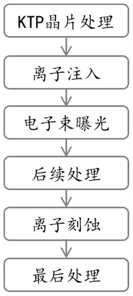
[0044] according to Figure 1-9 As shown, this embodiment proposes a method for preparing a KTP nonlinear racetrack-type microring resonator, including the following steps:

[0045] Step 1. KTP wafer processing

[0046] First, the surface of the cut and formed KTP wafer is polished, and after the polishing is completed, it is cleaned. After cleaning, it is placed in a storage device for storage and standby;

[0047] Step 2. Ion Implantation

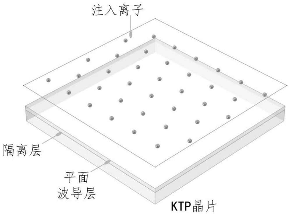
[0048] Take out the spare KTP wafer in step 1, and then use ion implantation equipment to implant the ions accelerated by the ion accelerator into the KTP wafer, such as figure 2As shown, an isolation layer with a reduced refractive index is formed at a depth of several microns below the surface of the KTP wafer, and the part above the isolation layer is a waveguide layer. In the second step, the type of ions is one of carbon ions or oxygen ions, In the second step, the range of several micrometers is 5-10 micrometers, and the prepara...

Embodiment 2

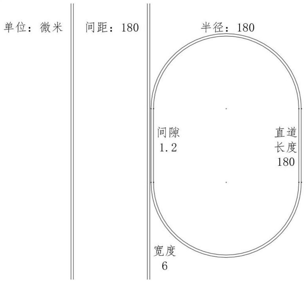
[0058] according to Figure 10 As shown, this embodiment takes the generation of frequency doubling (second harmonic) in the band around 1064 nanometers as an example, in which the attached Figure 10 The upper part of the figure is a schematic diagram of the 1064nm frequency doubling of the microring resonator. The arrows indicate the propagation direction of the light. When the KTP crystal undergoes appropriate phase matching processing (cut along a specific angle, such as θ=90°, φ=23.5°, when Class II phase matching can be achieved), which will meet the phase matching conditions of nonlinear frequency doubling.

[0059] At this time, when the 1064-nanometer laser passes through the straight waveguide, it will be coupled to the micro-ring resonator in the form of an evanescent wave (Evanescent Wave). The left and right frequency doubled light, the generated frequency doubled light will also be coupled into the straight waveguide in the form of an evanescent wave, and finall...


PUM

PropertyMeasurementUnit
thicknessaaaaaaaaaa

Abstract

The present invention proposes a method for preparing a KTP nonlinear racetrack microring resonator, including six steps of KTP wafer processing, ion implantation, electron beam exposure, follow-up processing, ion etching processing and final processing, through one process of ion implantation, Just realized the preparation of the thin-film waveguide structure similar to the on-chip lithium niobate thin-film material, the production process is greatly simplified, the time is shortened, and the cost is significantly reduced. At the same time, the KTP nonlinear microring resonator finally prepared by the present invention is compatible with existing Compared with Lithium Oxide nonlinear microring resonators, it has a higher optical damage threshold, which can increase the output power of nonlinear frequency conversion light from microwatts to milliwatts, and is suitable for both input and output optical signals. In the case of pulsed laser, ion implantation, electron beam exposure, metal evaporation deposition coating, and reactive ion etching are all relatively mature micro-nano processing technologies, making the present invention have good operability and repeatability.

Description

technical field [0001] The invention relates to the fields of ion beam material modification, Wiener processing and integrated optics, in particular to a method for preparing a KTP nonlinear racetrack type microring resonator. Background technique [0002] A microring resonator is a component of integrated optics that contains at least one closed annular optical path, in which light can circulate and reciprocate. Light of a specific wavelength, due to resonance in the microring resonator, is constructive interference, and continuously strengthen; [0003] At present, microring resonators are mostly used in silicon-based integrated optics, mainly based on silicon, silicon dioxide, silicon carbide and other materials. This is because the processing technology of silicon-based materials has been relatively complete and mature, and is widely used in silicon-based integrated circuits. Photolithography for semiconductor chip processing and subsequent reactive ion etching technolo...

Claims


Application Information

Patent Timeline
Patent Type & Authority Patents(China)
IPC IPC(8): G02B6/13G02B6/134G02B6/136G02B6/132G02F1/355G02F1/365
CPCG02B6/13G02B6/1347G02B6/136G02B6/132G02F1/3553G02F1/365G02B6/12007G02B6/29338G02B2006/12176
Inventor 陈琛韩张华
Owner SHANDONG NORMAL UNIV
Why Eureka
Try Eureka