System and method for monitoring and controlling temperature and optical power of optical waveguide device in situ

A device temperature, monitoring and control technology, applied in the direction of control/regulation system, temperature control, non-electric variable control, etc., can solve the problems of inaccurate monitoring of the actual temperature of the optical waveguide, inaccurate optical power of the optical waveguide, etc.

Active Publication Date: 2021-11-12
TIANJIN UNIV
View PDF8 Cites 0 Cited by
  • Summary
  • Abstract
  • Description
  • Claims
  • Application Information

AI Technical Summary

Problems solved by technology

[0007] When there is a temperature difference between the fixed position of the commercial temperature sensor and the integrated optical waveguide device, the commercial temperature sensor cannot accurately monitor the actual temperature of the optical waveguide; when the temperature of the optical waveguide changes, it will cause the optical waveguide obtained by CLIPP to monitor the change in admittance. The optical power of the waveguide is not accurate

Method used


Image

  • System and method for monitoring and controlling temperature and optical power of optical waveguide device in situ
  • System and method for monitoring and controlling temperature and optical power of optical waveguide device in situ
  • System and method for monitoring and controlling temperature and optical power of optical waveguide device in situ

Examples


Embodiment approach 1

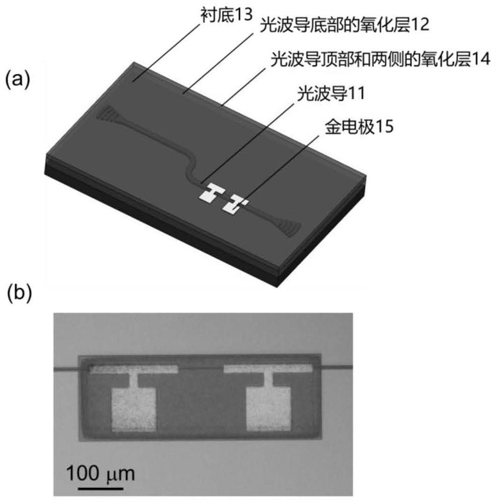
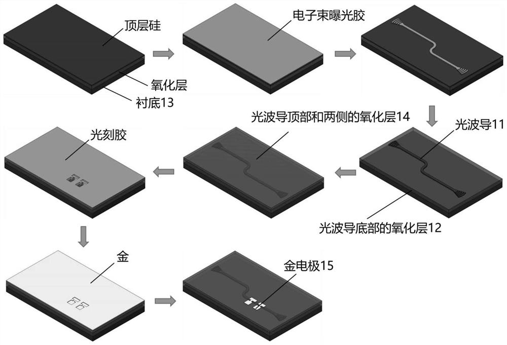
[0058] The processing flow chart of CLIPP 1 is as follows: figure 2 shown. First, the structure of the optical waveguide is defined by scanning electron beam exposure (SEBL), and the optical waveguide 11 is processed by transferring the electron beam exposure glue pattern to the device layer by inductively coupled plasma etching (ICP), and the residual glue after etching is removed by using an organic solvent ; Utilize ion-enhanced chemical vapor deposition (PECVD) to deposit silicon dioxide layer afterwards as the upper cladding of optical waveguide; Finally, utilize ultraviolet lithography to engrave gold electrode 15 patterns, utilize sputtering to deposit titanium gold, lift off in organic solvent , remove excess photoresist and metal, and process the titanium-gold electrode 15 .

Embodiment approach 2

[0060] When the optical power of the integrated optical waveguide device changes, the surface state absorption effect will cause the admittance of the optical waveguide to change; when the temperature of the integrated optical waveguide device changes, the temperature-induced changes in the number of carriers and mobility of the optical waveguide also Will cause the admittance of the optical waveguide to change. Based on the above properties of the optical waveguide, the temperature and optical power monitoring of the integrated optical waveguide device can be realized by using CLIPP 1.

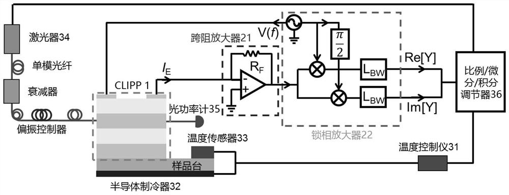
[0061] image 3 Schematic diagram of the device for simultaneous in-situ monitoring and control of the temperature and optical power of the integrated optical waveguide device. The lock-in amplifier 22 outputs a sinusoidal voltage signal with adjustable frequency. The signal is input through the titanium gold electrode at one end of CLIPP 1 and output from the titanium gold electrode at the ...

Embodiment approach 3

[0063] Simultaneous monitoring of temperature and optical power of integrated optical waveguide devices:

[0064] Measure the relationship between the change of admittance and the temperature and optical power at the driving frequency of 1MHz and 5MHz, and it can be obtained by linear interpolation Image 6 (a) The scanning diagram of the admittance variation of temperature and optical power under the two driving frequencies shown in (a). Measure the admittance change of the two driving frequencies of 1MHz and 5MHz at the same temperature and optical power, and form two constant admittance change planes, and then Image 6 The surface in (a) is intercepted, and the projection of the obtained two curves on the temperature-optical power plane (such as Image 6 (a) The intersection point corresponds to the temperature and optical power of the current integrated optical waveguide device, such as Image 6 (b) shown.


PUM

PropertyMeasurementUnit
thicknessaaaaaaaaaa
thicknessaaaaaaaaaa
thicknessaaaaaaaaaa

Abstract

The invention discloses a system and a method for monitoring and controlling the temperature and the optical power of an optical waveguide device in situ. The system comprises the steps of measuring the admittance variation of an optical waveguide at different frequencies through CLIPP, and simultaneously monitoring the optical power and the temperature of an integrated optical waveguide device in situ by combining with the function relation at different test frequencies; and enabling a feedback control circuit to feed back and control the temperature and the optical power of the integrated optical waveguide device according to the admittance variation obtained by a signal reading circuit. The method comprises the following steps: selecting a plurality of driving frequencies, and respectively fitting a binary function relationship among temperature, optical power and admittance variation; reading the admittance variation of the CLIPP under the driving frequencies, and reversely deducing the temperature and the optical power of the integrated optical waveguide device; using the temperature and the optical power, obtained by the signal reading circuit, of the integrated optical waveguide device, enabling a PID regulator to feed back and adjust the current provided for the TEC by the temperature controller and the output optical power of a laser, and adjusting the temperature and the optical power of the integrated optical waveguide device to set values.

Description

technical field [0001] The invention relates to the field of optoelectronic devices, in particular to a system and method for in-situ monitoring and controlling the temperature and optical power of an optical waveguide device. Background technique [0002] Integrated optical waveguide devices generally refer to optical devices with a single function made of semiconductor materials through micro-nano processing, including: directional couplers, arbitrary waveguide gratings, optical waveguide integrated detectors, micro-ring resonators, etc. The waveguide is the main body, the scale is on the order of nanometers or micrometers, and it can be integrated on a large scale. The integrated optical waveguide chip is composed of a variety of integrated optical waveguide devices to achieve specific functions, such as: routing, beam phase control, etc. [0003] Integrated optical waveguide devices require real-time temperature monitoring and temperature feedback control to ensure that...

Claims


Application Information

Patent Timeline
Patent Type & Authority Applications(China)
IPC IPC(8): G01D21/02G05D23/20
CPCG01D21/02G05D23/20
Inventor 胡小龙张子彧王昭邹锴
Owner TIANJIN UNIV
Why Eureka
Try Eureka