Ring gate nano CMOS structure and preparation method thereof
A nanometer and gate-around technology, which is applied in the manufacture of semiconductor/solid-state devices, electrical components, transistors, etc., can solve the problems of many steps, high cost and complicated technology in the manufacture of gate-around nanowires/sheet field effect transistors, and reduce the production cost. Cost and process difficulty, enhanced performance and reliability, effect of reduced process
- Summary
- Abstract
- Description
- Claims
- Application Information
AI Technical Summary
Problems solved by technology
Method used
Image

Examples
Embodiment 1
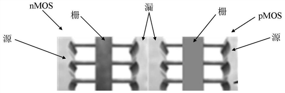
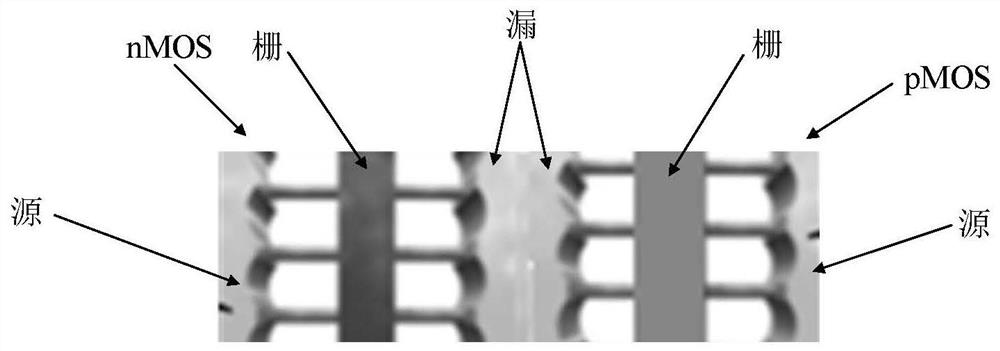
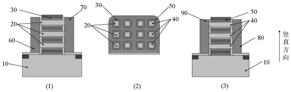
[0052] See image 3 , image 3 is a schematic diagram of a gate-all-around nano-CMOS structure provided by an embodiment of the present invention, wherein, image 3 (1), image 3 (3) is a sectional view of a side view, image 3 (2) is a partial sectional view of the front view. Based on the above reasons, the present embodiment provides a gate-all-around nano-CMOS structure, which includes nMOS and pMOS. The first gate electrode 30 of the structure 20, the pMOS includes a second nanobody structure 40 disposed on the semiconductor substrate 10 and a second gate electrode 50 surrounding the second nanobody structure 40, wherein the first nanobody structure 20 and the second nanobody structure The two nanobody structures 40 are formed of semiconductor materials of the same conductivity type; the first gate electrode 30 and the second gate electrode 50 are formed of conductive materials of the same work function. It should be emphasized that the thickness and doping concentra...
Embodiment 2
[0065] On the basis of the above-mentioned embodiments, this embodiment also provides a method for preparing a gate-all-around nano-CMOS structure. The method for preparing the gate-all-around nano-CMOS structure includes:
[0066] Step 2.1, selecting a semiconductor substrate 10;
[0067] Step 2.2, forming a first material stack and a second material stack on the semiconductor substrate 10;
[0068] Step 2.3, removing the sacrificial layer of the first material stack and the sacrificial layer of the second material stack to form the first nanobody structure 20 with the first source region 60 and the first drain region 70 at both ends, and A second nanobody structure 40 with a second source region 80 and a second drain region 90 disposed at both ends;
[0069] Step 2.4, forming a gate dielectric layer and a first gate electrode 30 and a second gate electrode 50 with the same work function around the first nanobody structure 20 and the second nanobody structure 40 to form nMOS...
Embodiment 3
[0089] See Figure 6a ~ Figure 6n , Figure 6a ~ Figure 6n It is a schematic diagram of the preparation process of stacking the same layer of gate-all-around nanowires / sheet CMOS provided by the embodiment of the present invention. Based on the above content, this embodiment also provides a preparation method of stacking the same layer of gate-all-around nanowires / sheet CMOS. The preparation method is illustrated by taking the nanowire / sheet (second material layer) as Si and the sacrificial layer (first material layer) as SiGe as an example. The preparation method includes:
[0090] Step 3.1, see Figure 6a , providing a semiconductor substrate 10 .
[0091] Specifically, semiconductor substrate 10 is bulk Si.
[0092] Step 3.2, epitaxially growing laminated materials.
[0093] The stacked material will be used to prepare nanowires / sheets of stacked gate-all-around nano-CMOS. The conductivity type of the stacked material can be n-type or p-type. According to the design req...
PUM
| Property | Measurement | Unit |
|---|---|---|
| electron work function | aaaaa | aaaaa |
| electron work function | aaaaa | aaaaa |
Abstract
Description
Claims
Application Information
 - R&D
- Intellectual Property
- Life Sciences
- Materials
- Tech Scout
- Unparalleled Data Quality
- Higher Quality Content
- 60% Fewer Hallucinations
Browse by: Latest US Patents, China's latest patents, Technical Efficacy Thesaurus, Application Domain, Technology Topic, Popular Technical Reports.
© 2025 PatSnap. All rights reserved.Legal|Privacy policy|Modern Slavery Act Transparency Statement|Sitemap|About US| Contact US: help@patsnap.com