Packaging material structure layer for front connection of high junction temperature power module chip and manufacturing method thereof

A technology for power modules and packaging materials, applied in the fields of semiconductor/solid-state device manufacturing, semiconductor/solid-state device components, semiconductor devices, etc., can solve the problems of low carrying capacity, unsuitability for industrialization, chip failure, etc., to reduce circuit failure The probability of , is conducive to mass production, the effect of increasing the thickness of the copper sheet

Active Publication Date: 2020-12-15
南瑞联研半导体有限责任公司
View PDF7 Cites 0 Cited by
  • Summary
  • Abstract
  • Description
  • Claims
  • Application Information

AI Technical Summary

Problems solved by technology

For high junction temperature working environment, ordinary bonding aluminum wires will fall off and disconnect, which will lead to premature failure of individual chips and affect the long-term reliability of the module
[0003] The mainstream bonding material of traditional power chips is aluminum bonding wire, the melting point of pure aluminum is 660 degrees Celsius, and the wire diameter ranges from 8 to 20 mils, but the wire diameter that is bonded to the chip to conduct current is mainly 15 mil (375um). ;The aluminum wire is connected to the front of the chip through ultrasonic vibration and friction through ultrasonic bonding equipment, and is used to connect the conduction current; however, the current carrying capacity of a single 15mil aluminum wire is about 10A, and the longer the arc, the lower the carrying capacity
In addition, the copper wire bonding on the front of the chip is an ideal material that can replace the aluminum wire bonding, but the hardness of the copper wire is more than twice that of the aluminum wire, and the Al and Ag metallization layers bonded to the traditional chip front are very easy Damage to the chip; some studies have shown that copper wire bonding can be achieved by performing copper metallization on the chip surface, but the formation of a copper metallization layer that can be effectively bonded takes a long time and is extremely expensive, and is not suitable for industrialization at present; The research institution invented the DTS technical solution. By using the sintered silver process to connect a certain thickness of copper thin film on the front of the chip, it can replace the production of copper metallization layer for copper wire bonding. At present, industrialization can be realized, but the cost of equipment and materials is relatively high; There are also research institutions that use Sn-based solder to connect thicker copper terminals on the front of the chip, or DBC to form an effective connection for the current on the front of the chip. However, Sn-based solder is suitable for ordinary chips, and the process is more complicated.
[0004] The current carrying capacity of a single aluminum wire bonded by aluminum wire is about 10A. The longer the arc is, the lower the carrying capacity is. When the device is short-circuited, the bonding wire cannot withstand the large current and fuses, resulting in a short circuit. In a high-voltage environment, it is easy to cause the module to explode.
In addition, the copper wire bonding on the front of the chip is an ideal material that can replace the aluminum wire bonding, but the hardness of the copper wire is more than twice that of the aluminum wire, and the Al and Ag metallization layers bonded to the traditional chip front are very easy Damage to the chip; some studies have shown that copper wire bonding can be achieved by performing copper metallization on the chip surface, but the formation of a copper metallization layer that can be effectively bonded takes a long time and is extremely expensive, and is not suitable for industrialization at present; The research institution invented the DTS technical solution. By using the sintered silver process to connect a certain thickness of copper thin film on the front of the chip, it can replace the production of copper metallization layer for copper wire bonding. At present, industrialization can be realized, but the cost of equipment and materials is relatively high; There are also research institutions that use Sn-based solder to connect thicker copper terminals on the front of the chip, or DBC to form an effective connection for the current on the front of the chip. However, Sn-based solder is suitable for ordinary chips, and the process is more complicated.

Method used


Image

  • Packaging material structure layer for front connection of high junction temperature power module chip and manufacturing method thereof
  • Packaging material structure layer for front connection of high junction temperature power module chip and manufacturing method thereof
  • Packaging material structure layer for front connection of high junction temperature power module chip and manufacturing method thereof

Examples


Embodiment Construction

[0027] The present invention will be further described below in conjunction with the accompanying drawings. The following examples are only used to illustrate the technical solution of the present invention more clearly, but not to limit the protection scope of the present invention.

[0028] The invention discloses a method for manufacturing a packaging material structure layer for front-side connection of high junction temperature power module chips, comprising the following steps:

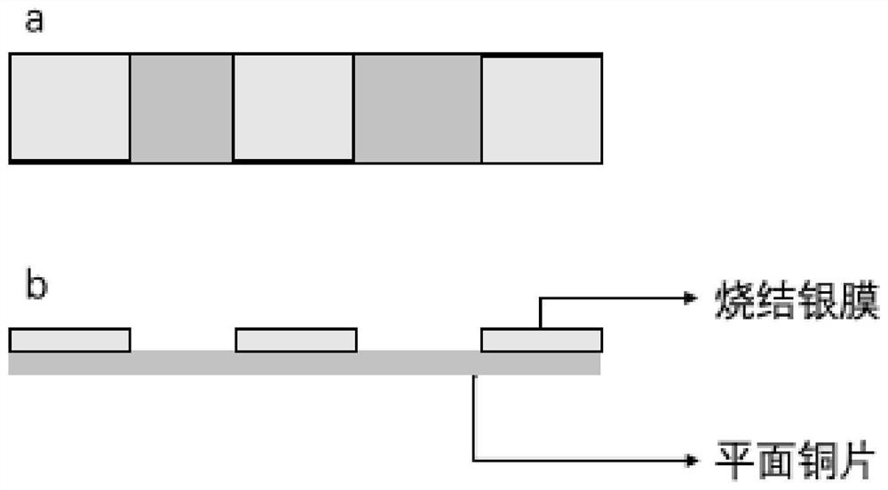
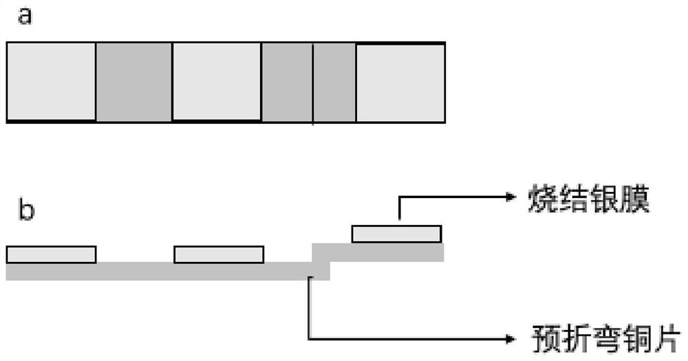
[0029] Step 1: Make a preformed planar single CSBT copper sheet or copper bar by stamping, mechanical cutting or laser cutting. The width is slightly smaller than the width of the metal pad on the front of the chip, and the thickness is 70-500 microns. The length can be based on the chip size of the package design. and interval design.

[0030] Step 2, if plating is required, silver, nickel, gold or other metal layers are plated on the copper sheets or copper bars. The chip front bonding materi...


PUM

PropertyMeasurementUnit
thicknessaaaaaaaaaa

Abstract

The invention discloses a manufacturing method of a packaging material structure layer for front connection of a high junction temperature power module chip, which comprises the following steps of: S01, manufacturing a preformed planar copper sheet or copper bar of which the width is smaller than that of a metal Pad on the front of the chip; S02, printing sintered silver paste on the surface of the copper sheet or the copper bar through a printing process to form a layer of silver film; and S03, curing the printed copper sheet or copper bar in an oven to form the copper sheet silver film composite material. The invention further provides a packaging material structure layer for front connection of the high junction temperature power module chip, and the packaging material structure layer is manufactured by the manufacturing method of the packaging material structure layer for front connection of the high junction temperature power module chip. According to the packaging material structure layer for front connection of the high junction temperature power module chip and the manufacturing method thereof, batch production is facilitated, the packaging material structure layer is usedfor front bonding of the high-junction-temperature power module chip, and the packaging material structure layer is applied to an application environment of the high-junction-temperature chip at the temperature of 400 DEG C or above.

Description

technical field [0001] The invention relates to a packaging material structure layer for front connection of high junction temperature power module chips and a manufacturing method thereof, belonging to the technical field of packaging of power semiconductor devices. Background technique [0002] The power module can withstand high voltage and provide high current, and is easy to control. It is an important power device for motor control and power inverter. The power chip is welded on the copper-clad ceramic board (DBC) with solder (solder paste or solder sheet), sintered silver, and the front side of the chip is conducted by aluminum wire bonding. In actual use, especially silicon carbide (SiC) chips and gallium nitride (GaN) chips with high junction temperature (greater than or equal to 300 degrees Celsius), a chip front bonding material with high temperature resistance and high elastic modulus is required; due to the working of IGBT The frequency is high, and the tempera...

Claims


Application Information

Patent Timeline
Patent Type & Authority Applications(China)
IPC IPC(8): H01L21/603H01L23/48
CPCH01L24/03H01L24/04H01L23/48H01L2224/03505H01L2224/04105H01L2224/05147H01L2224/05139H01L2224/40139H01L2224/40225H01L2224/32225H01L2224/84
Inventor 刘克明杨金龙骆健黄全全王立胡小刚臧传龙
Owner 南瑞联研半导体有限责任公司
Why Eureka
Try Eureka