Manufacturing method of silicon-based germanium detector with low dark current

The invention relates to a germanium detector and a manufacturing method, which can be applied to circuits, electrical components, semiconductor devices, etc., and can solve the problems of fast corrosion rate, difficulty in controlling germanium corrosion amount, influence of germanium doping concentration, etc., and achieve the effect of stable corrosion effect.

Active Publication Date: 2022-03-01
THE 44TH INST OF CHINA ELECTRONICS TECH GROUP CORP
View PDF9 Cites 0 Cited by
  • Summary
  • Abstract
  • Description
  • Claims
  • Application Information

AI Technical Summary

Problems solved by technology

However, due to the fast corrosion rate of germanium in the etchant and the influence of the doping concentration of germanium, it is difficult to control the amount of germanium corrosion in the actual process, and it is easy to cause excessive corrosion to make the geometric shape of the germanium detector deviate from the design value and affect its photoelectric parameters.

Method used


Image

  • Manufacturing method of silicon-based germanium detector with low dark current
  • Manufacturing method of silicon-based germanium detector with low dark current
  • Manufacturing method of silicon-based germanium detector with low dark current

Examples


Embodiment Construction

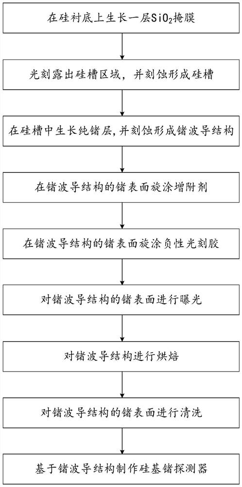
[0026] In order to enable those skilled in the art to better understand the technical solutions in the embodiments of the present invention, and to make the above-mentioned purposes, features and advantages of the embodiments of the present invention more obvious and understandable, the following describes the technical solutions in the embodiments of the present invention in conjunction with the accompanying drawings For further detailed explanation.

[0027] In the description of the present invention, unless otherwise specified and limited, it should be noted that the term "connection" should be understood in a broad sense, for example, it can be a mechanical connection or an electrical connection, or it can be the internal communication of two elements, it can be Directly connected or indirectly connected through an intermediary, those skilled in the art can understand the specific meanings of the above terms according to specific situations.

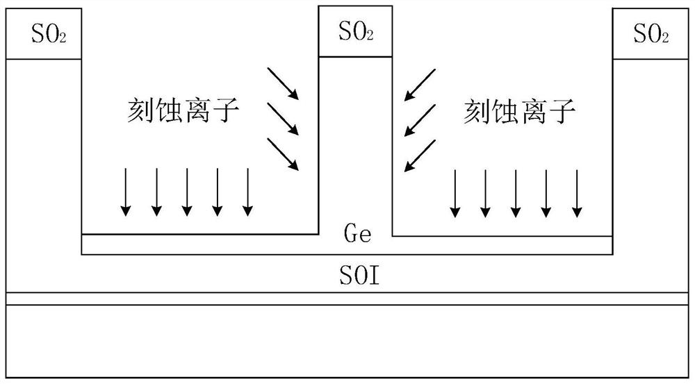
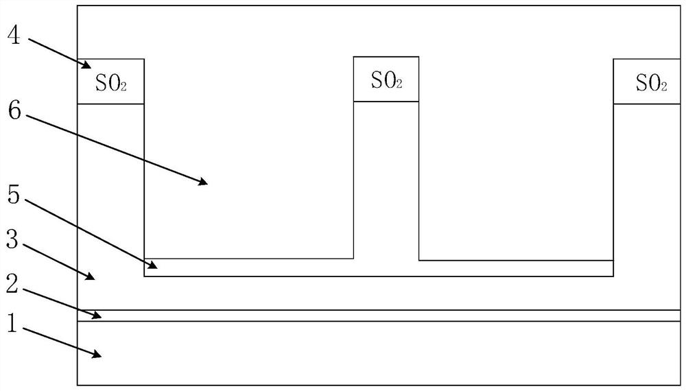
[0028] Such as figure 2 As...


PUM

PropertyMeasurementUnit
thicknessaaaaaaaaaa

Abstract

The invention discloses a method for manufacturing a silicon-based germanium detector with low dark current. First, a silicon groove is etched on a silicon substrate, a pure germanium layer is epitaxially grown in the silicon groove, and a waveguide structure is etched on the pure germanium layer. The germanium waveguide structure is formed by etching, and then the surface of the germanium waveguide structure is spin-coated with adhesion enhancer and negative photoresist, and sequentially exposed and baked; finally, the germanium surface is cleaned and made into a silicon-based germanium detector. In the present invention, after the germanium waveguide structure is formed, a negative photoresist is covered on the surface of the germanium material, and the germanium material is corroded by the slight oxidation of the negative photoresist to remove the etching damage layer on the germanium surface, thereby reducing the Dark current introduced by waveguide etching damage; since the negative photoresist mainly reacts with highly active defects such as dangling bonds on the surface of germanium, it has little corrosion to germanium, and only the damaged layer on the surface will be removed, and the rate is not high. Affected by the doping type of germanium, the corrosion effect is stable and will not affect the morphology of the germanium detector.

Description

technical field [0001] The invention relates to the field of silicon-based germanium detectors, in particular to a manufacturing method of a silicon-based germanium detector with low dark current. Background technique [0002] Silicon-based germanium detectors are waveguide detectors, such as figure 1 As shown, such detectors usually need to epitaxially grow a pure germanium layer on the SOI substrate, and complete the etching of the waveguide structure on the pure germanium layer, and then fabricate the germanium detector based on the structure of the germanium waveguide. The waveguide etching in the preparation of waveguide-type silicon-based germanium detectors can be dry-etched by reactive ion etching (RIE) etching machine. Reactive ion etching is etched by molecular gas plasma in a vacuum system, using ion Inducing chemical reaction to achieve anisotropic etching is to use ion energy to form an easily etched damaged layer on the surface of the etched layer and promote ...

Claims


Application Information

Patent Timeline
Patent Type & Authority Patents(China)
IPC IPC(8): H01L31/028H01L31/10H01L31/18
CPCH01L31/028H01L31/10H01L31/1808Y02P70/50
Inventor 刘恋高建威郭安然杨修伟刘鹏浩雷仁方
Owner THE 44TH INST OF CHINA ELECTRONICS TECH GROUP CORP
Why Eureka
Try Eureka