HEMT device based on Cu substrate and preparation method thereof
A substrate and device technology, applied in the field of HEMT devices, can solve problems such as thermal stability of HEMT devices, and achieve the effects of excellent crystal quality, small device leakage current, and stable performance
- Summary
- Abstract
- Description
- Claims
- Application Information
AI Technical Summary
Problems solved by technology
Method used
Image

Examples
Embodiment 1
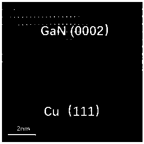
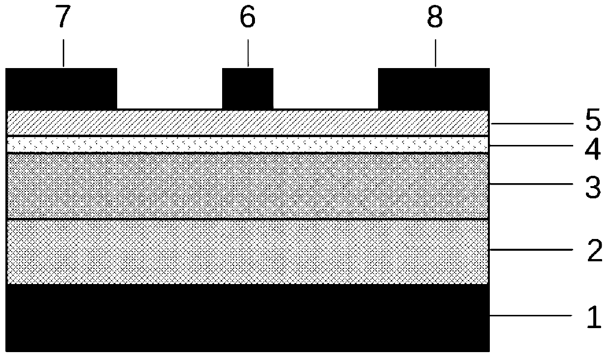
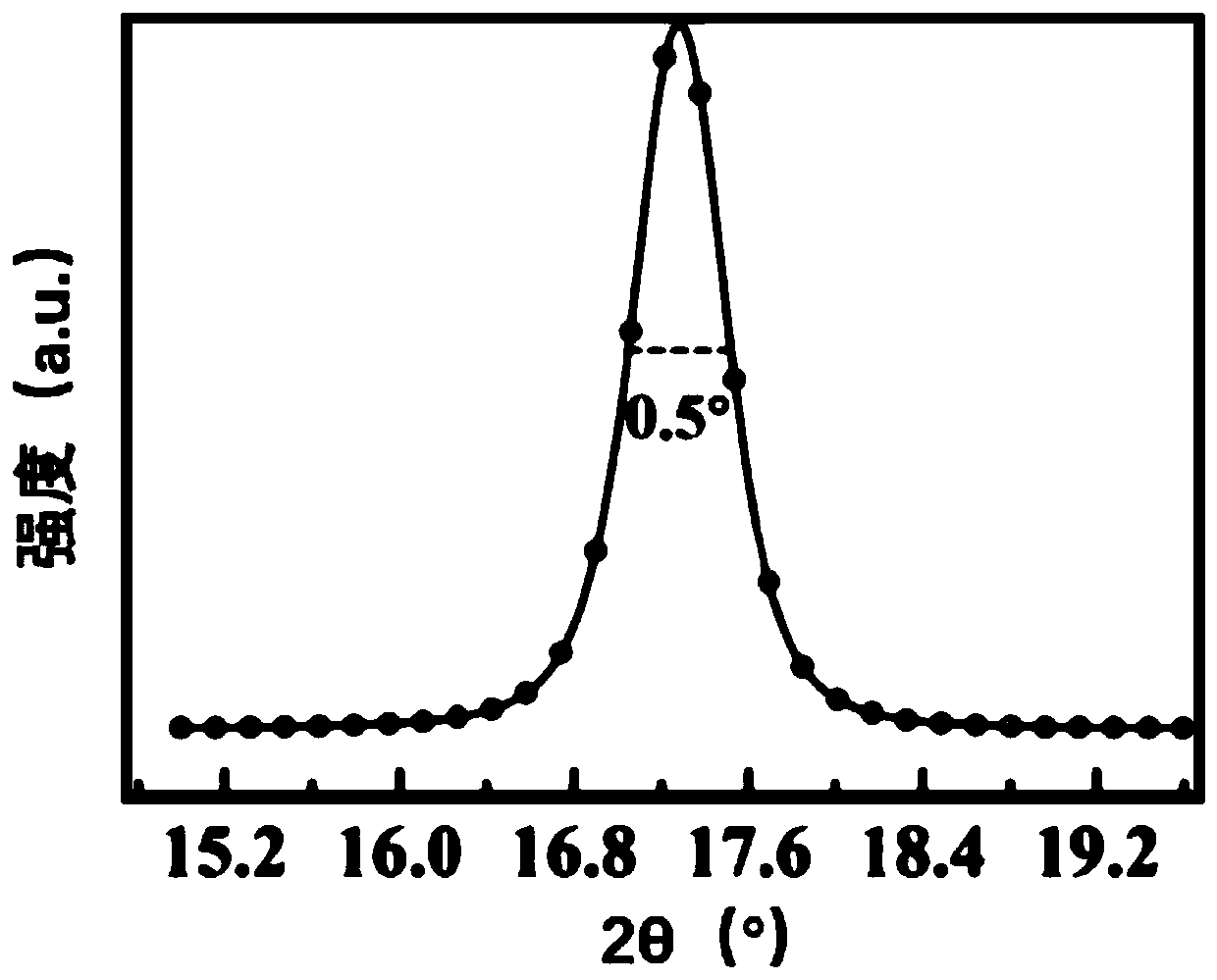
[0041] Step 1. At room temperature, clean and dry the single crystal Cu(111) substrate, put it into a rapid annealing furnace, pass in 25 sccm argon gas, and anneal at 400°C to obtain a clean single crystal Cu substrate, and into a pulsed laser deposition (PLD) chamber.
[0042] Step 2. Through the general process of electron beam evaporation, a graphite layer of 5 μm is selectively deposited on a 2-inch GaN target. The target area covered by the graphite layer and the target area not covered by the graphite layer are distributed axisymmetrically. The ratio is 2:1.
[0043]Step 3. Through the general process method of pulsed laser deposition (PLD), set the PLD laser energy to 380mJ, maintain the frequency at 20Hz, maintain the growth temperature at 600°C, maintain the distance between the target and the substrate at 4mm, and maintain the cavity pressure at 4mTorr , a 2 μm carbon-doped GaN high-resistance layer was sequentially grown on a Cu(111) substrate (the doping concentr...
Embodiment 2
[0047] Step 1. At room temperature, clean and dry the single crystal Cu(111) substrate, put it into a rapid annealing furnace, pass in 25 sccm argon gas, and anneal at 400°C to obtain a clean single crystal Cu substrate, and into a pulsed laser deposition (PLD) chamber.
[0048] Step 2. Through the general process of electron beam evaporation, a graphite layer of 5 μm is selectively deposited on a 2-inch GaN target. The target area covered by the graphite layer and the target area not covered by the graphite layer are distributed axisymmetrically. The ratio is 2.3:1.
[0049] Step 3. Through the general process method of pulsed laser deposition (PLD), set the PLD laser energy to 400mJ, maintain the frequency at 25Hz, maintain the growth temperature at 650°C, maintain the distance between the target and the substrate at 4.5mm, and maintain the cavity pressure at 4.5mTorr, a 3μm carbon-doped GaN high-resistance layer was sequentially grown on a Cu(111) substrate (the doping con...
Embodiment 3
[0053] Step 1. At room temperature, clean and dry the single crystal Cu(111) substrate, put it into a rapid annealing furnace, pass in 25 sccm argon gas, and anneal at 400°C to obtain a clean single crystal Cu substrate, and into a pulsed laser deposition (PLD) chamber.
[0054] Step 2. Through the general process of electron beam evaporation, a graphite layer of 5 μm is selectively deposited on a 2-inch GaN target. The target area covered by the graphite layer and the target area not covered by the graphite layer are distributed axisymmetrically. The ratio is 2.5:1.
[0055] Step 3. Through the general process method of pulsed laser deposition (PLD), set the PLD laser energy to 350mJ, maintain the frequency at 30Hz, maintain the growth temperature at 700°C, maintain the distance between the target and the substrate at 5mm, and maintain the cavity pressure at 5mTorr , a 4 μm carbon-doped GaN high-resistance layer was sequentially grown on a Cu(111) substrate (the doping conce...
PUM
| Property | Measurement | Unit |
|---|---|---|
| thickness | aaaaa | aaaaa |
| thickness | aaaaa | aaaaa |
| size | aaaaa | aaaaa |
Abstract
Description
Claims
Application Information
 - R&D
- Intellectual Property
- Life Sciences
- Materials
- Tech Scout
- Unparalleled Data Quality
- Higher Quality Content
- 60% Fewer Hallucinations
Browse by: Latest US Patents, China's latest patents, Technical Efficacy Thesaurus, Application Domain, Technology Topic, Popular Technical Reports.
© 2025 PatSnap. All rights reserved.Legal|Privacy policy|Modern Slavery Act Transparency Statement|Sitemap|About US| Contact US: help@patsnap.com