Femtosecond Laser Cutting Method of Silicon Carbide

A femtosecond laser, cutting method technology, applied in laser welding equipment, sustainable manufacturing/processing, final product manufacturing, etc., can solve the problems of long processing time, low cutting accuracy, large material loss, etc., to avoid cracks and damages , the preparation cycle is short, the effect of avoiding waste

Active Publication Date: 2022-02-08
BEIJING UNIV OF TECH
View PDF10 Cites 0 Cited by
  • Summary
  • Abstract
  • Description
  • Claims
  • Application Information

AI Technical Summary

Problems solved by technology

This method has relatively high requirements on the processing technology, long processing time, and strict control of the winding and stretching of the wire saw to ensure that the ingot is evenly stressed; at the same time, the material loss due to this method is relatively large, and the material cost is expensive. Under certain conditions, there is more than 50% material waste; and, this method is limited by the size of the wire saw, the cutting accuracy is low, and the wafer thickness is large; the most fatal thing is that this processing method must be carried out in a humid and polluted environment, and After cutting, the surface is rough, and it is necessary to introduce grinding, polishing and other processes that are labor-intensive and pollute the environment. It can be seen that the research on new technologies for silicon carbide wafer cutting is imminent

Method used


Image

  • Femtosecond Laser Cutting Method of Silicon Carbide
  • Femtosecond Laser Cutting Method of Silicon Carbide

Examples


Embodiment Construction

[0015] Below in conjunction with embodiment further illustrate the present invention, but the present invention is not limited to this embodiment.

[0016] The invention discloses a femtosecond laser cutting method for silicon carbide, which specifically includes the following steps:

[0017] 1) Ultrasonic the SiC wafer in alcohol for 15 minutes, dry it naturally and fix it on the three-dimensional precision processing table;

[0018] 2) The laser beam (wavelength 800nm, pulse width 130fs-150fs, repetition rate 1000Hz, average power 725mW, single pulse energy 0.725mJ, spot radius 2mm) produced by the femtosecond laser is adjusted by a beam expander collimator and focused (f= 30mm) onto the SiC wafer on the processing table;

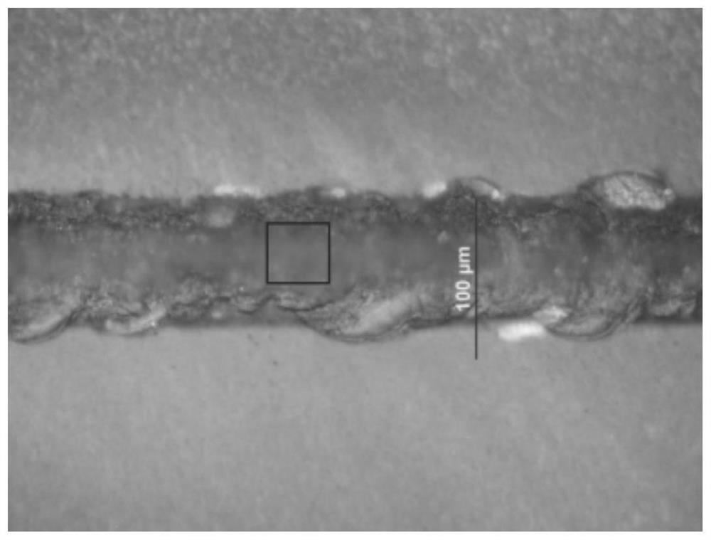
[0019] 3) Set the movement rate of the three-dimensional precision machining table to 3mm / s, so that the SiC wafer is scanned by the femtosecond laser at the focal plane in a single pass to realize cutting. Raman spectra of wafers before and after dicin...


PUM

PropertyMeasurementUnit
Mohs hardnessaaaaaaaaaa

Abstract

The invention discloses a femtosecond cutting method of silicon carbide. A femtosecond laser with a specific intensity is used to scan a silicon carbide wafer once to break silicon carbide molecular bonds, thereby realizing the purpose of cutting. Ultrasonic the SiC wafer in alcohol to remove dust and oil on the surface, dry it and fix it on a three-dimensional processing table; femtosecond laser with a wavelength of 800nm, a pulse width of 130fs‑150fs, a repetition rate of 1000Hz, an average power of 725mW, and a single pulse energy of 0.725mJ , the spot radius is 2mm; through the adjustment of the beam expander and collimator, the focus is on the SiC wafer on the processing table through the lens with a focal length of 30mm and the back and forth movement of the 3D platform; by controlling the movement of the 3D processing table in the horizontal direction, the Precise cutting of SiC wafers by femtosecond laser. The invention has the advantages of precise cutting, material saving, simple process, no pollution, good repeatability and the like.

Description

technical field [0001] The invention belongs to the technical field of semiconductors, and in particular relates to a method for cutting silicon carbide, a third-generation semiconductor substrate material, by using a femtosecond laser. Background technique [0002] The third-generation semiconductor technology represented by wide bandgap materials SiC and GaN has led the development of new energy, intelligent manufacturing, information technology and other fields in recent years. In the future, with the commercialization of 5G and the development of artificial intelligence , The needs of green cities will bring greater development space for the third-generation semiconductor technology. However, the hardness of silicon carbide material is extremely high, with a Mohs hardness of 9.5, which is second only to the world's hardest diamond (grade 10), and it is not easy to cut. Existing cutting method is wire saw cutting. When cutting, wrap the steel wire saw around the silicon...

Claims


Application Information

Patent Timeline
Patent Type & Authority Patents(China)
IPC IPC(8): H01L21/268B23K26/38B23K26/402B23K26/70
CPCB23K26/38B23K26/402B23K26/70Y02P70/50
Inventor 窦菲门慧婕张新平
Owner BEIJING UNIV OF TECH
Why Eureka
Try Eureka