Cavity type bulk acoustic wave resonator without preparing sacrificial layer and preparation method of cavity type bulk acoustic wave resonator

A bulk acoustic wave resonator and sacrificial layer technology, applied in electrical components, impedance networks, etc., can solve the problems of cavity corrosion residues and low film quality, and achieve the effects of high yield, less damage, and reduced clutter.

Active Publication Date: 2019-07-05
CHIMEMS MICROELECTRONICS CO LTD
View PDF5 Cites 9 Cited by
  • Summary
  • Abstract
  • Description
  • Claims
  • Application Information

AI Technical Summary

Problems solved by technology

[0005] The invention provides a cavity-type bulk acoustic resonator without preparing a sacrificial layer and its preparation method to solve the problem of low film quality and corrosion in the cavity when preparing a cavity-type thin-film bulk acoustic resonator in the prior art. residue problem

Method used


Image

  • Cavity type bulk acoustic wave resonator without preparing sacrificial layer and preparation method of cavity type bulk acoustic wave resonator
  • Cavity type bulk acoustic wave resonator without preparing sacrificial layer and preparation method of cavity type bulk acoustic wave resonator
  • Cavity type bulk acoustic wave resonator without preparing sacrificial layer and preparation method of cavity type bulk acoustic wave resonator

Examples


Embodiment 1

[0055] The method for preparing a cavity-type BAW resonator without preparing a sacrificial layer in this embodiment includes the following steps:

[0056] (a) Take a piezoelectric single crystal wafer, the piezoelectric single crystal wafer is a lithium tantalate wafer, perform ion implantation on the piezoelectric single crystal wafer to form an ion damage layer, and the implanted ions are H ions , the energy of implanted ions is 195KeV, and the implantation dose is 6×10 16 / cm 2 , the ion beam current is 1μm / cm- 2 , the implantation depth is 6 μm to obtain a pyroelectric material, and then photolithography forms a pattern to be grown on the injection surface of the obtained pyroelectric material, and then utilizes magnetron sputtering to grow electrodes, the electrode material is Au, and finally passes through acetone Wash off the excess part to obtain a piezoelectric single crystal wafer with ion implantation and a bottom electrode, the thickness of the bottom electrode ...

Embodiment 2

[0070] The method for preparing a cavity-type BAW resonator without preparing a sacrificial layer in this embodiment includes the following steps:

[0071] (a) Take a piezoelectric single crystal wafer, the piezoelectric single crystal wafer is a lithium tantalate wafer, perform ion implantation on the piezoelectric single crystal wafer, the implanted ions are As ions, the energy of the implanted ions It is 150KeV-1000KeV; the implantation depth is 0.5-1.8μm to obtain a pyroelectric material, and then grow an electrode on the injection surface of the obtained pyroelectric material by magnetron sputtering, the electrode material is Au, and then prepare a mask , and finally etch off the excess part to obtain a piezoelectric single crystal wafer that has undergone ion implantation and has a bottom electrode, and the thickness of the bottom electrode is 100 nm;

[0072] (b) Take the piezoelectric single crystal wafer having the bottom electrode through ion implantation, and form a...

Embodiment 3

[0077] The preparation method of the cavity-type bulk acoustic wave resonator in this embodiment without preparing a sacrificial layer is prepared by the same method as that of Embodiment 1, except that the upper surface area of ​​the bottom electrode is larger than the upper surface area of ​​the cavity.

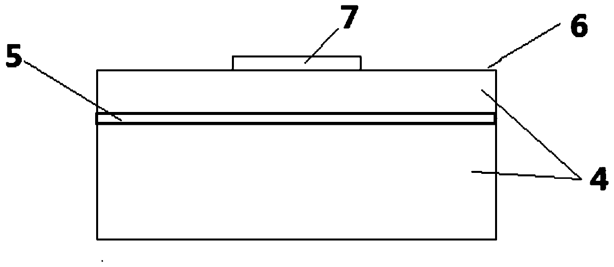
[0078] Such as Figure 8 Shown is a structural schematic diagram of the ion-implanted piezoelectric single crystal wafer obtained in step (b) and having a bottom electrode.

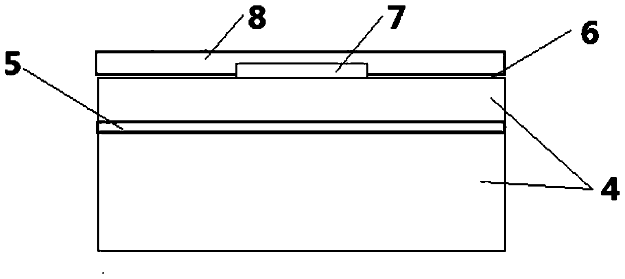
[0079] Figure 9 It is a schematic structural diagram of the piezoelectric single crystal wafer described in step (c) of the method for preparing a cavity-type bulk acoustic resonator without preparing a sacrificial layer in Example 3 of the present invention after growing a supporting layer;

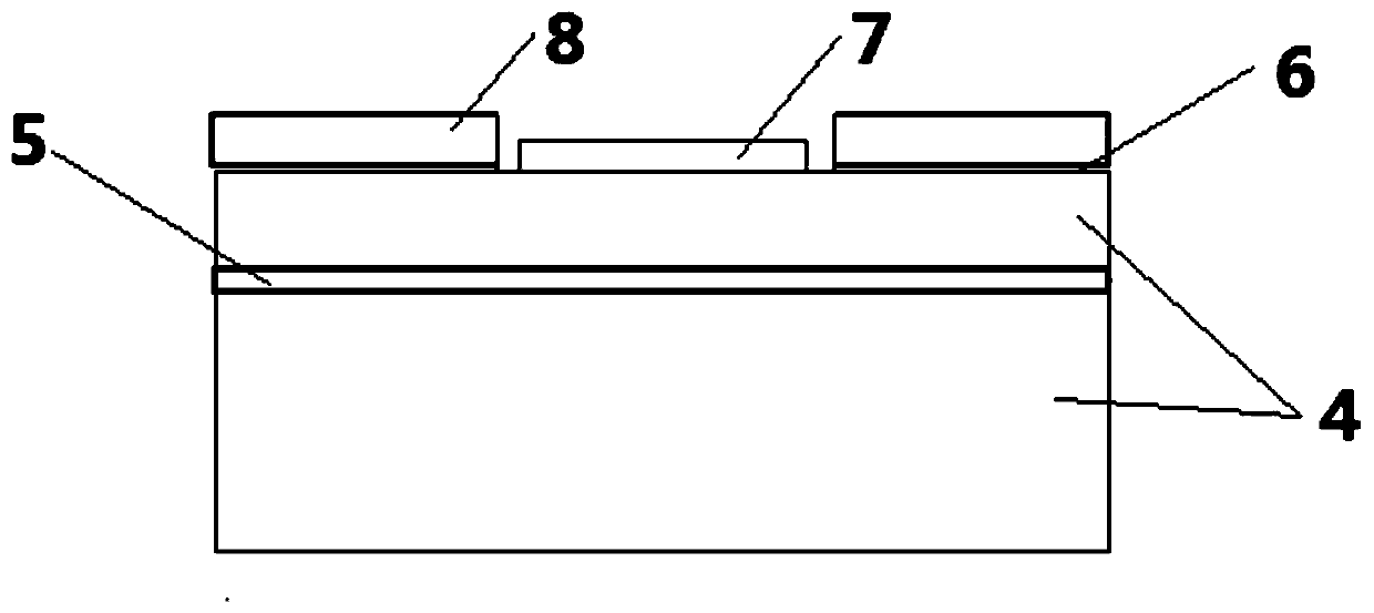
[0080] Figure 10 It is a schematic structural diagram of a cavity-type bulk acoustic resonator that does not need to prepare a sacrificial layer in step (d) of the method for preparing a cavity-type bulk acou...


PUM


Abstract

The invention provides a cavity type bulk acoustic wave resonator without preparing a sacrificial layer and a preparation method of the cavity type bulk acoustic wave resonator. The method comprises the following steps that a piezoelectric single crystal wafer which is subjected to ion implantation and provided with a bottom electrode is taken, a cavity is formed in the side, provided with the bottom electrode, of the piezoelectric single crystal wafer, then a substrate is taken, and the substrate and the side, provided with the cavity, of the piezoelectric single crystal wafer are bonded; andheat treatment is carried out on the bonded intermediate product to strip the film of the piezoelectric single crystal wafer, and then a top electrode is produced on one stripped side of the piezoelectric single crystal wafer to obtain the cavity type bulk acoustic wave resonator. According to the preparation method of the cavity type bulk acoustic resonator without the need of preparing the sacrificial layer, the sacrificial layer does not need to be grown, etching and trepanning are not carried out on the thin film, the mechanical strength of the device is improved, and damage to the thin film is not likely to be generated; the cavity structure is formed before film formation, the rate of finished products is high, residues left by etching after film formation do not exist, and the influence of incomplete release on the device does not need to be considered.

Description

technical field [0001] The invention belongs to the technical field of single crystal thin film devices, in particular, the invention relates to a cavity-type bulk acoustic wave resonator without preparing a sacrificial layer and a preparation method thereof. Background technique [0002] Film Bulk Acoustic Wave Resonator (FBAR) is a single crystal thin film device. In recent years, with the improvement of processing technology and the rapid development of wireless communication, due to its high Q value (greater than 1000) and the advantages of being compatible with the CMOS process have been developed rapidly. It converts electrical energy into sound waves through the inverse piezoelectric effect of the piezoelectric film to form resonance. The resonant cavity of the film bulk acoustic resonator is supported by a piezoelectric film, which is a sandwich structure in which the piezoelectric film is sandwiched between two metal electrodes. related to thickness. Both sides o...

Claims


Application Information

Patent Timeline
Patent Type & Authority Applications(China)
IPC IPC(8): H03H3/02H03H9/02H03H9/17
CPCH03H3/02H03H9/02015H03H9/02086H03H9/171H03H2003/023H03H2003/021H03H9/173
Inventor 帅垚吴传贵罗文博
Owner CHIMEMS MICROELECTRONICS CO LTD
Why Eureka
Try Eureka