
Method for manufacturing hot insertion application gold fingers

A manufacturing method and technology for gold fingers, which are applied in chemical/electrolytic methods to remove conductive materials, reinforce conductive patterns, and form electrical connection of printed components, etc. Liquid infiltration and other problems, to achieve the effect of sufficient dwell time, short curing time and low residual glue rate

Active Publication Date: 2019-06-18
CHANGSHU MUTUAL TEK CO LTD
View PDF5 Cites 0 Cited by
  • Summary
  • Abstract
  • Description
  • Claims
  • Application Information

AI Technical Summary

Problems solved by technology

However, in the existing technology, due to the selection and improper operation of anti-plating ink or blue glue, and the problem of liquid infiltration during etching, it often leads to uneven pitch between gold fingers or bleed-through phenomenon, which leads to an increase in product defect rate

Method used


Image

  • Method for manufacturing hot insertion application gold fingers
  • Method for manufacturing hot insertion application gold fingers

Examples


Embodiment 1

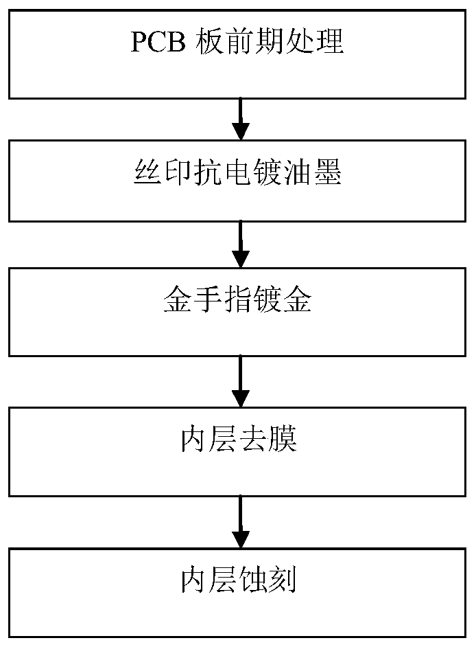
[0040] like figure 1 As shown, a method for making a gold finger for hot insertion in the present invention includes the following steps:

[0041] 1) Pre-treatment of the PCB board, setting a solder mask and sandblasting treatment on the PCB board;

[0042] 2) Silk-screen anti-plating ink, silk-screen anti-plating ink on the gold finger area and after exposure and development, cover the gold finger guide line part in the circuit board;

[0043] 3) The gold finger is gold-plated, the whole board is pasted with blue glue and the window is opened in the gold finger area for gold-plated treatment;

[0044] 4) the inner layer removes the film, and removes the wet film formed by the anti-plating ink;

[0045] 5) Inner layer etching, etch to remove the gold finger wires.

[0046] Wherein, the blue glue includes the following components by weight: 35 parts of vinyl acetate resin, 16 parts of alkyd resin, 20 parts of epoxy resin, 9 parts of acrylate monomer, 2.5 parts of light curin...

Embodiment 2

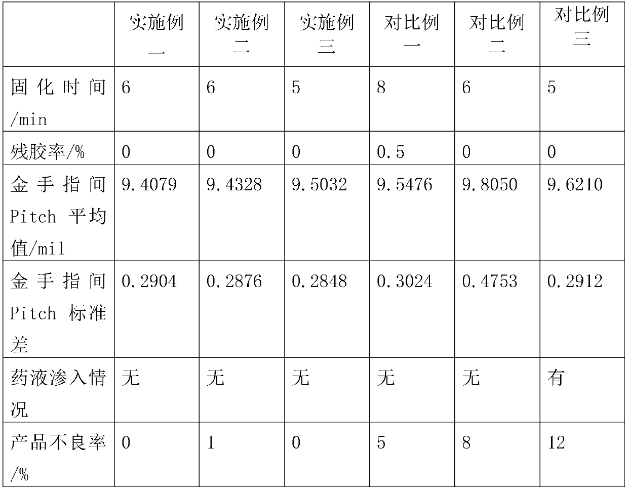
[0049] The difference between this embodiment and Embodiment 1 is that the blue glue includes the following components by weight: 40 parts of vinyl acetate resin, 14 parts of alkyd resin, 18 parts of epoxy resin, 9 parts of acrylate monomer, and 2.8 parts of curing agent, 1.5 parts of thixotropic agent, 4.5 parts of pigment, 0.4 part of cellulose acetate butyrate, 8 parts of nano calcium sulfate whiskers, 2 parts of butyl benzyl phthalate; the rest are the same as in Example 1.

Embodiment 3

[0051] The difference between this embodiment and Embodiment 1 is that the blue glue includes the following components by weight: 38 parts of vinyl acetate resin, 15 parts of alkyd resin, 19 parts of epoxy resin, 10 parts of acrylate monomer, light 2.7 parts of curing agent, 1.4 parts of thixotropic agent, 4.0 parts of pigment, 0.45 parts of cellulose acetate butyrate, 9 parts of nano-calcium sulfate whiskers, 1.5 parts of butyl benzyl phthalate, and the light curing agent is isopropyl Thioxanthone; All the other are identical with embodiment one.


PUM

PropertyMeasurementUnit
Thicknessaaaaaaaaaa
Thicknessaaaaaaaaaa

Abstract

The invention discloses a method for manufacturing hot insertion application gold fingers, comprising the following steps: 1) pre-processing of a PCB board, providing a solder mask layer on the PCB board and performing sand blasting treatment; 2) screen printing of anti-plating ink; 3) gold plating of gold fingers; 4) film removal of the inner layer, fading a wet film formed by the anti-plating ink; and 5) etching of the inner layer. After the wet film formed by the anti-plating ink in the invention is exposed and developed, the Pitch average value between the obtained gold fingers is closer to the design requirement, the standard deviation is smaller from the statistical point of view, that is, the Pitch flatness between the gold fingers is better; in addition, the blue glue in the invention is used, so that the curing time is shorter, and the residual glue rate is lower, the blue glue is filled at an electrogilding gold pinch point after gold plating of the gold fingers is completed,it is ensured that the standing time from etching of the inner layer to film removal of the inner layer is enough, such that the electroplating chemical can be prevented from infiltrating from the pinch point, thereby further reducing the defect rate of the product.

Description

technical field [0001] The invention relates to the field of printed circuit boards, in particular to a method for manufacturing gold fingers for hot insertion applications. Background technique [0002] Gold finger refers to the connection part formed on the circuit board to connect the slot. It is generally composed of many golden-yellow conductive contacts. Because the surface is gold-plated and the conductive contacts are arranged like fingers, they are also called gold fingers. In practical applications, the gold fingers are generally formed by coating a layer of gold on the copper clad board through an electroplating or chemical plating process. However, in the prior art, due to the selection and improper operation of anti-plating ink or blue glue, as well as the problem of liquid infiltration during etching, it often leads to uneven pitch between gold fingers or seepage phenomenon, resulting in an increase in product defect rate. Contents of the invention [0003] ...

Claims


Application Information

Patent Timeline
IPC IPC(8): H05K3/40H05K3/24H05K3/06
Inventor 林睦群
Owner CHANGSHU MUTUAL TEK CO LTD
Learn More