Semiconductor transistor structure and preparation method thereof

A semiconductor and transistor technology, applied in the field of semiconductor transistor structure and its preparation, to achieve the effect of reducing the value of parasitic capacitance

Pending Publication Date: 2019-02-26
CHANGXIN MEMORY TECH INC
View PDF9 Cites 7 Cited by
  • Summary
  • Abstract
  • Description
  • Claims
  • Application Information

AI Technical Summary

Problems solved by technology

[0003] Metal-oxide-semiconductor field-effect transistor (MOSFET) structure is widely used in the process layout of semiconductor integrated circuits (IC). In the MOSFET structure, a sidewall insulating layer must be formed on the sidewall to isolate the plug conductive layer from the gate conductive layer. layer, so as to avoid the short circuit of the two conductor layers from causing the failure of the device (Device), but it also generates parasitic capacitance
As the process of DRAM (Dynamic Random Access Memory) continues to shrink to the nanometer level, it is a big challenge to improve the parasitic capacitance between the gate and the contact conductor under the condition of greatly shrinking the device

Method used


Image

  • Semiconductor transistor structure and preparation method thereof
  • Semiconductor transistor structure and preparation method thereof
  • Semiconductor transistor structure and preparation method thereof

Examples


Embodiment 1

[0066] see Figure 2a-2m , the preparation method of the semiconductor transistor structure provided in this embodiment includes the following steps:

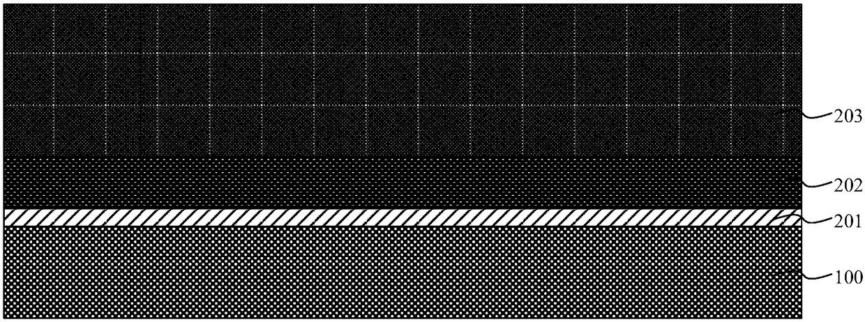
[0067] S11 as Figure 2a As shown, a gate dielectric layer 201 , a gate conductive layer 202 and an insulating protection layer 203 are sequentially formed on a semiconductor substrate 100 . Specifically, the semiconductor substrate 100 can be a silicon substrate; an oxide layer can be oxidized on the surface of the silicon substrate as the gate dielectric layer 201, with a thickness of 1-10 nm; A 60nm tungsten metal conductive film and a 50-300nm thick silicon nitride film are used as the gate conductive layer 202 and the insulating protection layer 203 respectively.

[0068] S12 as Figure 2b As shown, a gate pattern is defined, and a gate component is formed on the semiconductor substrate 100 by photolithography, and the gate component includes a gate dielectric layer 201, a gate conductive layer 202 on the gate dielectri...

Embodiment 2

[0080] see Figures 3a-3e , the preparation method of the semiconductor transistor structure provided in this embodiment includes the following steps:

[0081] S21 sequentially forming a gate dielectric layer 201 , a gate conductive layer 202 and an insulating protection layer 203 on the semiconductor substrate 100 .

[0082] S22 defines a gate pattern, and forms a gate component on the semiconductor substrate 100 by photolithography, and the gate component includes a gate dielectric layer 201, a gate conductive layer 202 on the gate dielectric layer 201, and An insulating protection layer 203 located on the gate conductive layer 202 .

[0083] S23 Form the first isolation layer 301, the sacrificial layer 302' and the second isolation layer 303 sequentially from the inside to the outside on the side wall of the gate assembly; the first isolation layer 301, the sacrificial layer 302', the second isolation layer 303, and etch to remove excess material after each vapor depositi...


PUM


Abstract

The present invention provides a semiconductor transistor structure and a preparation method thereof. The structure comprises: a semiconductor substrate; a grid module located on the semiconductor substrate, wherein the grid module comprises a grid dielectric layer and a grid conductive layer located on the grid dielectric layer; a side wall isolation structure located at the side wall of the gridmodule, wherein the side wall of the grid module comprises a first isolation layer, an air insulation layer and a second isolation layer arranged in order from inside to outside; and bolt conductivelayers located at two sides of the grid module, wherein the side wall isolation structure is configured to separate the bolt conductive layers from the grid module. The semiconductor transistor structure and the preparation method thereof can effectively reduce the stray capacitance value so as to improve the resistance-capacitance delay increasing speed and reduce the switching energy.

Description

technical field [0001] The invention relates to the field of integrated circuit manufacturing, in particular to a semiconductor transistor structure and a preparation method thereof. Background technique [0002] With the rapid development of integrated circuit technology, the density of devices in integrated circuits is getting higher and higher, and the feature size of semiconductor devices is continuously reduced, especially the shortening of effective gate length and short-channel effect (Short-channel effect). The leakage problem caused by channel effects, the hot carrier effect (Hot carrier effect) and other problems pose challenges to the reliability of the device. [0003] Metal Oxide Semiconductor Field Effect Transistor (MOSFET) structure is widely used in the process layout of semiconductor integrated circuits (IC). In the structure of MOSFET, it is necessary to form a side wall insulating layer on the side wall to isolate the plug conductive layer from the gate c...

Claims


Application Information

Patent Timeline
Patent Type & Authority Applications(China)
IPC IPC(8): H01L29/78H01L29/51H01L21/336
CPCH01L29/515H01L29/6656H01L29/78
Inventor 不公告发明人
Owner CHANGXIN MEMORY TECH INC
Why Eureka
Try Eureka