
Liquid crystal display for eliminating movable mura

a liquid crystal display and mura technology, applied in non-linear optics, instruments, optics, etc., can solve the problems of reducing the transmission ratio of the panel, light leakage, and the relative shift between the array substrate and the color filter substrate can easily occur, so as to prevent the decrease of the aperture ratio and eliminate the mura phenomenon.

Active Publication Date: 2017-08-22
TCL CHINA STAR OPTOELECTRONICS TECH CO LTD
View PDF7 Cites 2 Cited by
  • Summary
  • Abstract
  • Description
  • Claims
  • Application Information

AI Technical Summary

Benefits of technology

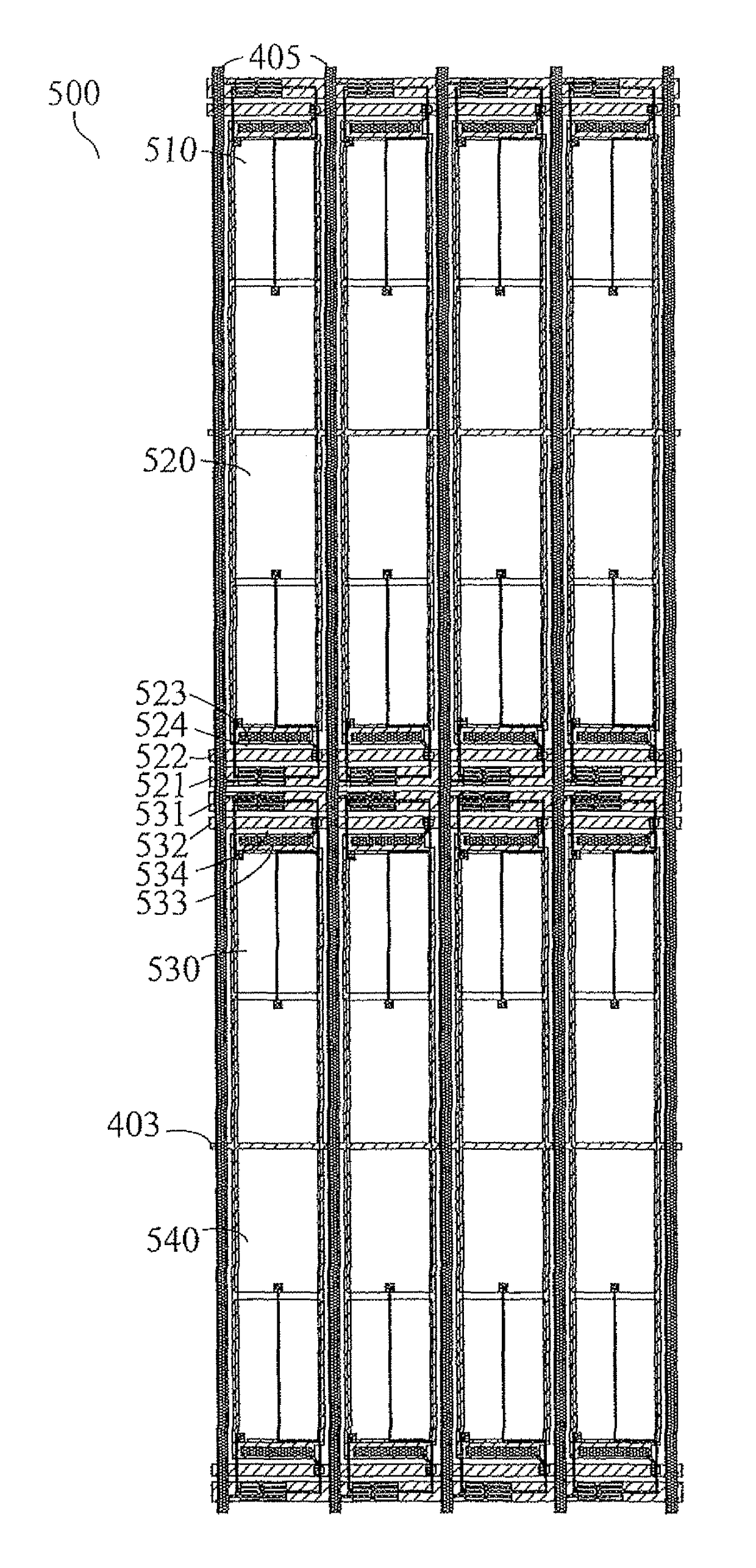
The present invention provides an array substrate and liquid crystal display device that can improve the aperture ratio and reduce the movable mura phenomenon. Additionally, it also decreases the RC delay of the data line and increases the power rate of the pixels. This is achieved by arranging pixel units in rows and sharing capacitors between adjacent pixel units. The arrangement of the gate line groups of adjacent pixel units and the sharing capacitors helps to separate light leakage regions and maximize the aperture ratio of the pixel unit. The present invention also decreases the intersection number of data line and common electrode line, which results in a half reduction in parasitic capacitance and decreased cost of extra wiring.

Problems solved by technology

However, in practice, a relative shift between the array substrate and the color filter substrate can easily occur because these two substrates are attached to each other by using adhesive at the edges of the panel in a vertical alignment liquid crystal display.
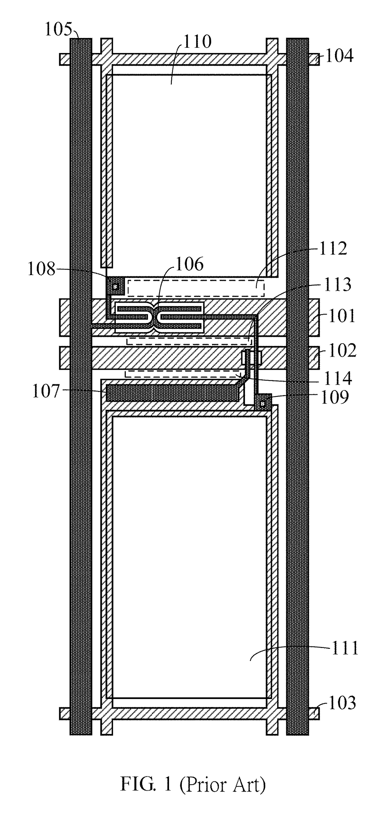
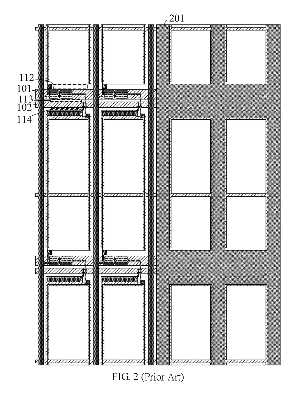
However, when an upward shift of the color filter substrate with respect to the array substrate occurs, a light leakage will not occur as long as the length of the shift is less than the width of the sharing capacitor 107, but when a downward shift takes place on the color filter substrate to the array substrate, even a small shift can cause light leakage.
Yet the drawback of above-mentioned solution is that the panel aperture ratio decreases as the width of the black matrix 201 increases, thereby decreasing the transmission ratio of the panel.

Method used


Image

  • Liquid crystal display for eliminating movable mura
  • Liquid crystal display for eliminating movable mura
  • Liquid crystal display for eliminating movable mura

Examples


first embodiment

[0025]FIG. 5 depicts a schematic diagram of a pixel unit layout as the present invention. The pixel units are arranged in a plurality of rows along the extending direction of the data line 405 on the substrate 500. Two adjacent pixel units are arranged sequentially in the opposite direction. In other words, the pixel units 510, 520, 530 and 540 are up-and-down sequentially arranged. With such a configuration, the charging gate lines 521 and 531 of the two adjacent pixel units 520 and 530 will be close to each other side by side and be gathered at the pixel junction, the sharing gate lines 522 and 532 with the sharing capacitors 523 and 533 of these two adjacent pixel units will also be gathered together at the pixel junction. Further, by using each of the sharing capacitors 523 and 533 of the two adjacent pixel units 520 and 530, the light leakage regions 523 and 534 below the corresponding sharing gate lines 522 and 532 will naturally be apart from the openings of the pixel electro...

second embodiment

[0026]With such, a configuration, in accordance with the present invention, the adjacent two pixel units 530 and 540 which their charging gate lines are apart from each other can share the same common electrode line 403. The intersection number of data line 405 and common electrode line 403 will therefore decrease by half, which means that the parasitic capacitance value of the data line and the common electrode line will decrease to half. Referring to FIG. 6, compared with the prior art array substrate 602, the array substrate 601 of the present invention has less RC delay. Thus, not only can the RC delay be effectively decreased and the pixel power rate enhanced, but the cost of extra wiring can also be decreased.

[0027]The present invention also relates to a liquid crystal display that comprises: an any substrate as shown in the first embodiment to the second embodiment of the present invention; a color filter substrate disposed opposite the array substrate; and a liquid crystal l...

third embodiment

[0028]FIG. 7 depicts the present invention, wherein the color filter substrate further comprises a black matrix 701 disposed on the corresponding data line 405; charging gate lines 721 and 731; sharing capacitors 723 and 733, and the common electrode line 403 of the array substrate for shielding the light leakage among each pixel unit. The above mentioned data line 405, charging gate lines 721 and 731, sharing capacitors 723 and 733, and the common electrode line 403 are opaque metal components, so that the aperture ratio will not decreased by the arrangement of the black matrix 701.

[0029]Since the pixel units arranged in a plurality of rows along the extending direction of the data line 405, two adjacent pixel units are arranged sequentially in the opposite direction. Therefore, the charging gate lines 721 and 731 of the two adjacent pixel units 720 and 730 will be close to each other side by side and be gathered at the pixel junction, the sharing gate lines 722 and 732 with the sh...


PUM

PropertyMeasurementUnit
widthaaaaaaaaaa
widthaaaaaaaaaa
color shiftaaaaaaaaaa

Abstract

An array substrate is disclosed. A gate line group, common electrode line and two adjacent data lines together defining a pixel unit which has: a thin film transistor; a first and second pixel electrode disposed between the gate line group and the common electrode line; a sharing capacitor disposed between the gate line group and the pixel electrodes. The pixel units are arranged in a plurality of rows along the extending direction of data line, two adjacent pixel units are arranged sequentially in opposite direction. By using each of the sharing capacitors of the adjacent pixel units, the light leakage regions will be away from the openings of the pixel electrodes, therefore the movable mura can be eliminated without increasing the width of the black matrix and the aperture ratio loss can be solved.

Description

FIELD OF THE INVENTION[0001]The present invention relates to a pixel array substrate and a liquid crystal display thereof. In particular, a pixel unit for eliminating movable mura in vertical alignment liquid crystal displays.BACKGROUND OF THE INVENTION[0002]In recent years, to eliminate the movable mura phenomenon in vertical alignment (VA) liquid crystal displays, the pixel unit of liquid crystal displays have adopted a charge-sharing technique to improve color shift at large viewing angle. Referring to FIG. 1, a charging gate 101, a sharing gate 102, and a common electrode line 103 and 104 are disposed on a first metal layer. A data line 105, a thin film transistor 106, and a sharing capacitor 107 are disposed on a second metal layer. Components of the first metal layer and components of the second metal layer are electrically connected to each other through contact holes 108 and 109. A pixel electrode layer disposed on the pixel array substrate fowls an opening, allowing light p...

Claims


Application Information

Patent Timeline
Patent Type & Authority Patents(United States)
IPC IPC(8): G02F1/1343G02F1/1362G02F1/1368G02F1/1335
CPCG02F1/136213G02F1/1368G02F1/13439G02F1/133514G02F1/134309G02F1/136286G02F1/13624G02F1/133512G02F2001/134345G02F1/134345
Inventor ZHENG, HUA
Owner TCL CHINA STAR OPTOELECTRONICS TECH CO LTD
Learn More