Polymer, electron injection layer, OLED device and display device
A technology of electron injection layer and polymer, which is applied in the direction of electric solid-state devices, lighting devices, electrical components, etc., can solve the problems of inability to print electron injection layer, reduce manufacturing cost, and high evaporation temperature, so as to reduce preparation cost and improve production efficiency. ability, the effect of reducing the interface barrier
- Summary
- Abstract
- Description
- Claims
- Application Information
AI Technical Summary
Problems solved by technology
Method used
Image

Examples
preparation example Construction
[0062] The invention provides a kind of preparation method of above-mentioned polymer, comprises the following steps:
[0063] Aromatic dihalides and any one of the compounds shown in formula (7) to formula (12) undergo a Suzuki reaction to obtain the polymer described in the above technical scheme;
[0064]
[0065] Among them, R 1 is H or acyloxy, R 2 , R 3 , R 4 Respectively selected from hydrogen, straight chain alkyl or branched chain alkyl containing 1 to 24 carbon atoms, or straight chain alkoxy or branched chain alkoxy containing 1 to 24 carbon atoms; R 5 For the borate group.
[0066] The preparation method is specifically:
[0067] Aromatic dihalides, any one compound shown in formula (7) ~ formula (12) and alkali are mixed uniformly in a solvent, and Suzuki reaction occurs under the action of palladium catalyst, then through concentration and separation, to obtain unit A and B A polymer formed by alternating copolymerization of units.
[0068] The molar ra...
Embodiment 1
[0154] 1. Synthesis of Monomer Benzenethiol-2,5-bis(cyclopropaneboronate)
[0155]Weigh 2,5-dibromobenzenethiol (2.66g, 10mmol) into a reaction flask, add anhydrous tetrahydrofuran solution under nitrogen protection, place the reaction flask in a dry ice and acetone bath, and drop the temperature to -78°C , a solution of n-butyllithium in n-hexane (1.6M, 7.2ml, 12mmol) was slowly added dropwise thereto. After reacting for 45 minutes, trimethyl borate (2.75 g, 26.7 mmol) was injected with a syringe, and then the reaction solution was gradually raised to room temperature and stirred for 12 hours. After the reaction of the raw materials was completed, the reaction system was placed in an ice-water bath to reduce to 0° C., stirred, and then a dilute sulfuric acid solution (2N, 50 ml) was slowly added dropwise, and the stirring was stopped after the dropwise addition was completed. At this time, the reaction system was divided into two phases, water and oil, and the oil phase was ...
Embodiment 2
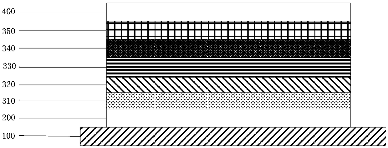
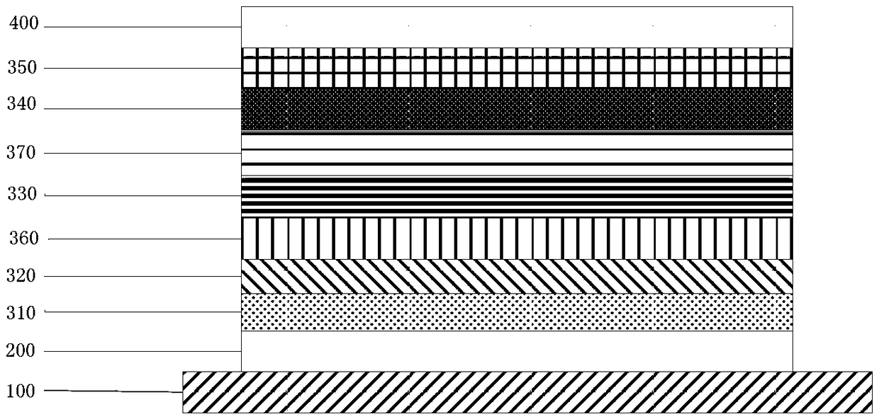
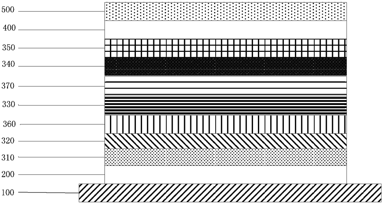
[0165] 1. Provide a substrate (both rigid and flexible), on which there is an array of thin film transistors required for driving and compensating the OLED, and a metal anode ITO / Ag / ITO is prepared on the array substrate, through exposure and development, Processes such as etching form the desired pattern, and there is an inkjet-printed pixel-defining layer on top of the anode.
[0166] 2. Spin coating or inkjet printing to form hole injection layer, hole transport layer, light emitting layer, electron transport layer and electron injection layer.
[0167] a) The anode modification layer is formed by spin coating, that is, the hole injection layer. The hole injection layer is a PEDOT:PSS film, which has the advantages of high electrical conductivity, good environmental stability and high transmittance. The main function is Modify the ITO anode, reduce the probability of device short circuit and reduce the turn-on voltage of OLED, etc. The preparation method of the thin film i...
PUM
| Property | Measurement | Unit |
|---|---|---|
| thickness | aaaaa | aaaaa |
| thickness | aaaaa | aaaaa |
| thickness | aaaaa | aaaaa |
Abstract
Description
Claims
Application Information
 - R&D
- Intellectual Property
- Life Sciences
- Materials
- Tech Scout
- Unparalleled Data Quality
- Higher Quality Content
- 60% Fewer Hallucinations
Browse by: Latest US Patents, China's latest patents, Technical Efficacy Thesaurus, Application Domain, Technology Topic, Popular Technical Reports.
© 2025 PatSnap. All rights reserved.Legal|Privacy policy|Modern Slavery Act Transparency Statement|Sitemap|About US| Contact US: help@patsnap.com